
Electronics are great for performing fast calculations, while photonics are ideal for moving information. A major drawback of the latter, however, is the slow and costly development process of new photonic integrated chips, preventing their widespread use. If photonic chips could be reprogrammed for different applications, this would greatly reduce development costs, shorten time-to-market, and increase the sustainability of their use.
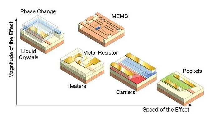
Caption: Various methods are ranked according to the speed of the relative movement efficiency they enable and their relative large movements. Low power consumption, low loss, short optical path and small size will be provided. A stronger mechanical communication requires a smaller area product or length to contain the phase shift.
To function, reprogrammable photonic chips require a large number of highly efficient electro-optic actuators to switch, split and filter the light signals passing through them. By introducing microelectromechanical systems (MEMS) and liquid crystal-based solutions, researchers are now developing low-power building blocks for large-scale and reconfigurable photonic integrated circuits (PICs). This versatile photonic chip is expected to accelerate applications in various industries, including biosensing, medical technology and information processing.
Innovation bottleneck
Over the past five years, we have witnessed a true electronics revolution. Electronics now power many basic activities in society. Photonic technology is now accelerating to experience a similar boom. Emerging PICs are increasingly important for powering today’s communications networks and data centers. At the same time, the complexity of these components is growing rapidly. A single photonic chip now has tens or even hundreds of thousands of building blocks.
However, in contrast to the electronic chip world where off-the-shelf chips can be purchased and programmed to perform various functions in various applications, most PICs are application-specific. The circuits that define the light paths on the chip are set up during the design phase for optimal performance of a specific function and manufactured as designed. This makes reprogramming inflexible and almost impossible to repurpose photonic chips for different purposes. Instead, each new application requires a new chip design.
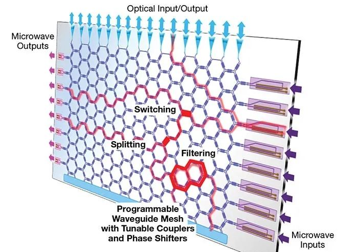
Caption: Programmable photonic circuit. The optical flow on the chip is controlled by a network of optical gates composed of tunable couplers and movers. Distributed on different roads, various functions can be implemented, including wavelength filters.
The design, manufacturing and testing cycle of photonic chips is slow and costly. It can easily take 12 months to know the outcome of a chip manufacturing run. And because the photonics ecosystem is not as mature as the electronics ecosystem, the chips made don’t always work as expected, especially in the first iterations of very complex circuits.
So, depending on the goals and the number of chip iterations needed to succeed, it could easily take five to six years to turn an idea into a real product. This time scale poses a huge barrier to entry for innovators who want to bring photonic chip technology into new applications. Today, PICs are primarily used in telecom and datacom environments. While there have been exciting demonstrations of PICs in sensing, spectroscopy, lidar, and quantum information processing, the number of actual commercial PIC-based products in these various application areas is still in the single digits.
One possible solution to break this deadlock and lower the barrier to entry is to introduce programmability into photonic circuits.
We can look again at the electronics example. Multipurpose programmable electronics, such as field-programmable gate arrays (FPGAs), have been a key enabler of innovation in consumer electronics. Photonics requires chips with a similar usage model: buy a generic off-the-shelf chip, then configure it to perform the desired optical function. Programmable photonic chips like this could cut the prototyping time for new photonic products from years to months or even weeks. This will greatly facilitate the use of photonic chips and the diversity of their applications.

Caption: LCD driver. Silicon rails next to the waveguides act as electrodes to redirect the liquid crystals in the gap. This causes a phase shift of the light passing through the waveguide. Liquid crystals are locally deposited into small cavities on the chip using inkjet printing (top). To characterize the phase shifter, it is embedded in one arm of an unbalanced Mach-Zehnder interferometer (bottom).
Ghent University, imec and other organizations are working on a collaborative project to create such universally programmable photonic chips. Like specialized chips, they face a new set of challenges.
To make an on-chip optical path configurable, it is necessary to incorporate hundreds of thousands of optical gates controlled by electrically tunable phase shifters. These phase shifters can induce tiny delays in the various paths of light, which then cause constructive or destructive interference of the light waves and cause optical signals to change their paths. The light gate thus acts as a microscopic switch coupling two inputs and two outputs, with the added ability to continuously adjust the light separation from 0% to 100%, and also provides control over the light phase. This total control comes at a price: These basic building blocks need to behave really well, because light has to pass through a long chain of phase shifters.
MEMS and Liquid Crystals
The traditional way to implement light gates on photonic chips is to use tiny heaters. These are tiny electric heaters located near the waveguide. Heating the waveguide changes its optical properties, causing a phase shift. Although these heaters are very small, they each dissipate many milliwatts of power, making scaling to very large circuits difficult.
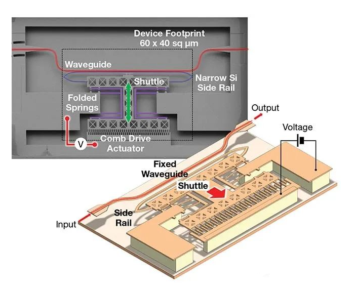
MEMS optical phase shifter. Silicon (Si) waveguides are flanked by thin silicon rails. All elements are suspended. The rail can be pulled away from the waveguide using electrostatic forces in the comb drive actuator. When the silicon track is farther away from the waveguide, the light in the waveguide will register less silicon nearby and travel faster, causing a phase shift.
In 2018, the EU-funded MORPHIC project was launched to enhance programmable silicon photonic circuits with advanced waveguide MEMS. MEMS are small mechanical actuators, only a few microns in size, that can change the distance between two waveguides. These movable waveguides can be driven electrostatically, simply by maintaining a voltage across a capacitor. There is no static power consumption to maintain the state of the device. The optical effects of MEMS phase shifters are very strong. Physically moving the silicon structure enables the device to produce very large changes in the light-perceived optical environment.
The MORPHIC consortium demonstrated MEMS phase shifters and tunable waveguide couplers with a length of only 60 µm and power consumption levels in the nanowatt range. While this is not the first time a MEMS actuator has been combined with an optical waveguide, MORPHIC demonstrates the first integration of MEMS into a complete silicon photonics platform without sacrificing the performance of other key components on the platform, such as high-speed modulators and germanium photodetectors device.
This integration is not simple. Traditional silicon photonic waveguides are encapsulated in a cladding of silicon dioxide and other dielectrics, and the movable waveguide components must be freestanding, meaning they are suspended in air or a vacuum. A team of six European partners, including MORPHIC, solved this problem by partially removing the support layer beneath the waveguide to make it removable, and then using a wafer-level hermetic sealing method to protect the free-standing MEMS device. As a result, these devices can be connected into larger circuits and connected to custom-designed multi-channel drivers and readout electronics using high-density insertion technology. From wafer-level processing through packaging and programming, the researchers demonstrated that these waveguide MEMS actuators can be used as efficient optical tuning mechanisms on silicon photonic chips. This achievement required a multidisciplinary effort involving semiconductor processing; electrical, optical, and mechanical design capabilities; and the development of multiple packaging and assembly processes and software routines.
In parallel to the MEMS approach, researchers are also exploring the potential of liquid crystals in programmable photonic chips. Liquid crystal materials are birefringent, which means they can change the index of refraction by using local electric fields to reorient liquid crystal molecules.
Under two grants from the European Research Council, researchers in the projects PhotonICSWARM and LIQUORICE have succeeded in integrating liquid crystals onto fully functional silicon photonic chips by locally embedding waveguides in the liquid crystal cladding. Light in the waveguide records localized rotations of the liquid crystal molecules, which can be driven with nearby electrodes. The resulting 50-μm-long phase shifter allowed the researchers to achieve a 0.8-π shift, driven by only 5 V and dissipating only a few microwatts.
An ideal phase shifter would consume very little power, have low optical losses, and have a footprint with minimal optical length. It would also help if the phase shifters offered very fast nanosecond response times and could be controlled using CMOS compatible voltages. Meeting all these requirements is very difficult, and so far, no such ideal phase shifter has been demonstrated. But recent collaborative research on liquid crystals and MEMS devices offers two promising candidates, and researchers are using these new phase shifters to enable larger programmable circuits.
Complete technology stack
Programmable photonics is more than a network of light gates on a chip. Each of these actuators must be connected to drive electronics, which must be controlled through multiple layers of software using monitoring signals collected from on-chip photodiodes. All of these must be integrated using a combination of optical, electrical, thermal and mechanical packaging techniques. To realize the potential of programmable photonics, all elements of the technology stack must be covered.
MORPHIC completed its goal in 2022, but the consortium is starting a new chapter in the follow-up project PHORMIC. The team brought in additional partners to help address another critical aspect of building large-scale programmable silicon photonic chips: integrating transfer-printed optical amplifiers and light sources onto the same chip.
Amplifiers can help overcome accumulated optical losses in larger circuits, but they also offer the possibility of designing programmable light sources on the chip itself.
The overall goal of the two projects is to develop a photonic platform on which a single chip can be used to demonstrate various optical functions, such as modulating or demodulating different optical communication formats, reading out optical sensor signals or for spectroscopic applications. Combined with onboard high-speed modulators and detectors, this chip-based platform can also implement microwave functions, which will be valuable for next-generation 6G wireless communication networks.
The ability to prototype different functions using the same chip could be a game-changer in the PIC space as it enables the same kind of rapid development model that has proven so successful in electronic product development.
Valencia, Spain-based startup iPronics recently announced that it has commercialized the first of its kind operational photonic processors, to much fanfare. This achievement demonstrates that the optoelectronics industry is on the right path to achieve wider adoption and innovation in photonic integrated chips.
Post time: Apr-27-2023