
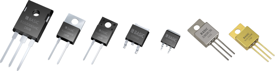
The latest silicon carbide device production and mass production situation and downstream terminal application progress analysis
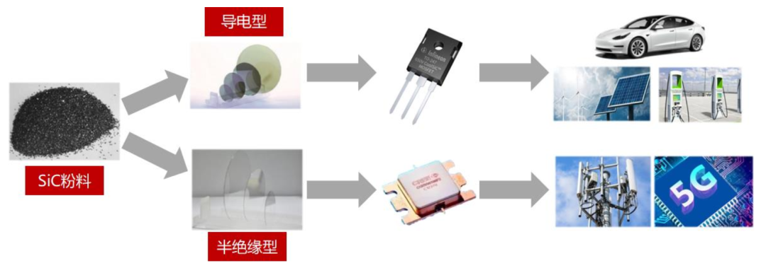
Silicon carbide, with the chemical formula SiC, is a compound semiconductor material composed of carbon and silicon elements. It is one of the ideal materials for making high-temperature, high-frequency, high-power, and high-voltage devices. Silicon carbide devices refer to devices made of silicon carbide as the raw material. According to different resistance properties, they are divided into conductive silicon carbide power devices and semi-insulating silicon carbide-based radio frequency devices.
Conductive silicon carbide power devices are mainly made by growing silicon carbide epitaxial layers on conductive substrates to obtain silicon carbide epitaxial wafers and further processing. The varieties include Schottky diodes, MOSFETs, IGBTs, etc., and are mainly used in electric vehicles. , Photovoltaic power generation, rail transit, data centers, charging and other infrastructure. Semi-insulating silicon carbide-based radio frequency devices are further manufactured by growing gallium nitride epitaxial layers on semi-insulating silicon carbide substrates to obtain silicon carbide-based gallium nitride epitaxial wafers, including HEMT and other gallium nitride radio frequency devices. Mainly used in 5G communication, vehicle communication, defense application, data transmission, aerospace.
Technical difficulties in large-scale application of silicon carbide
The silicon carbide industry chain mainly includes substrates, epitaxy, device design, manufacturing, packaging and testing and other links. Upstream is substrate and epitaxy, midstream is device and module manufacturing, and downstream is end application.
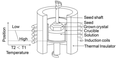
Although the silicon carbide substrate and device technology are gradually mature, the prices of substrates and devices show a certain downward trend, but the current price of silicon carbide power devices is still several times that of silicon-based devices, which limits the power of silicon carbide devices to a certain extent in the short term. Penetration in the device field. Cost has become a difficult problem for the large-scale application of silicon carbide devices, and the cost reduction process of silicon carbide devices needs to face many technical difficulties. Technical difficulty 1: The growth of silicon carbide substrates is “slow”. There are three main difficulties in the aspect of silicon carbide single crystal: high requirements on temperature and pressure control, and its growth temperature is above 2300°C; slow crystal growth rate, about 2cm silicon carbide ingots can be grown in 7 days; high crystal form requirements , The yield rate is low, and only a few types of single crystal silicon carbide with crystal structure can be used as semiconductor materials.
Technical Difficulty 2: The processing of silicon carbide substrates is “difficult”. The processing of silicon carbide single crystal is mainly divided into slicing, thinning and polishing. The global silicon carbide manufacturing and processing technology and industry are not yet mature, which limits the development of the silicon carbide device market to a certain extent. To fully realize the excellent performance of silicon carbide substrates, the development and improvement of silicon carbide wafer processing technology is the key.
Technical Difficulty Three: Silicon carbide defect density removal process barrier is “high”. There is a temperature gradient in the thermal field of silicon carbide single crystal growth, which leads to the existence of native internal stress and the resulting defects such as dislocations and stacking faults during the crystal growth process, and its reliability has attracted much attention. Orderly arrangement of atoms and crystal growth in a closed high-temperature chamber, while controlling micropipe density, dislocation density, resistivity, warpage, surface roughness and other parameters are complex system engineering, involving a series of difficult processes Regulation and high technological barriers. The technical path for cost reduction of silicon carbide devices, from the perspective of market dynamics, mainly includes three directions: expanding the wafer size, improving the silicon carbide growth process and improving the slicing process.
Expand wafer size. According to the latest information from Wolfspeed, from 6-inch to 8-inch wafers, the number of silicon carbide chips (32mm2) is expected to increase from 448 to 845, an increase of 75%. The basal and threaded screw densities of the 8-inch SiC substrate are 684 cm-2 and 289 cm-2, respectively. After chemical mechanical polishing, the surface quality was improved with 66 defects. SiC epitaxy can achieve thickness and doping uniformity of just over 1 %. According to GTAT’s estimate, compared with the 6-inch wafer platform, it is expected that the introduction of 8-inch substrates will reduce the overall cost of silicon carbide devices by 20-35%. Moreover, the thickness of the 6-inch SiC crystal is 350 microns, while the thickness of the 8-inch SiC substrate initially put on the market is 500 microns. Although the crystal cost will increase slightly, it is expected to further reduce the device production cost because thicker crystals can cut out more substrate slices. Improve silicon carbide crystal growth technology to increase crystal growth speed. On August 5, 2021, Sumitomo’s official website mentioned that they used a so-called MPZ technology to grow high-quality, low-cost SiC substrates and SiC epitaxial wafers, eliminating surface defects and basal dislocations (BPD), without The defect area (DFA) reaches 99%. Compared with the PVT method, the SiC crystal growth speed is increased by about 5 times, and compared with the ordinary LPE method, the speed is increased by 200 times.

Sumitomo MPZ (multi-parameter and zone control) solution growth technology
ColdSplit technology splits SiC wafers, thereby doubling the number of chips on a single wafer. ColdSplit technology divides silicon carbide wafers, thereby doubling the number of chips on a single wafer On November 12, 2018, Infineon Technologies AG acquired the start-up company Siltectra GmbH in Dresden. The start-up has developed an innovative technology (ColdSplit) for efficient processing of crystalline materials while minimizing material loss. Siltectra has developed a new technology for breaking down crystalline materials that reduces material loss to a minimum compared to ordinary sawing techniques. The technology is also applicable to carbon SiC and will be produced industrially at its existing plant in Dresden, as well as at Infineon’s (Austria) Villach plant.
The latest silicon carbide device production capacity progress
From the perspective of the global SiC device market share, STMicroelectronics has a market share of 40%, ranking first, followed by Infineon with a 22% market share. In terms of SiC production capacity, the production capacity of domestic companies in terms of substrate and epitaxy is mainly 4 inches, transitioning to 6 inches, while 6 inches has been commercialized internationally, and leading companies have started 8 inches layout, and domestic production capacity is still lagging behind. Domestic substrate end (Tianke Heda, Tianyue advanced), epitaxial end (Han Tiancheng) manufacturers have deployed 6-inch SiC, and device-end manufacturers are also developing 6-inch SiC chip production lines.
The latest developments in SiC device products of domestic manufacturers. From the perspective of application fields, STAR, BYD, and Times have already applied SiC modules in the field of new energy vehicles. Among them, Times Electric has SiC chip products covering all voltage levels. The price comparison of SiC devices of various companies shows that the higher the device is, the higher the price is. The average price of SiC diodes reaches double digits, and the average price of SiC MOSFET modules is even as high as thousands of yuan, mainly due to the combined price of multiple SiC diodes and a single SiC MOSFET in the module. Domestic manufacturers Tyco Tianrun and Star Semiconductor have deployed silicon carbide devices, showing an order of magnitude higher price advantage than silicon-based devices. In terms of SiC diodes, the average price of domestic manufacturer Tyco Tianrun reached 11 yuan/piece, higher than the average price of ordinary silicon-based diodes; in terms of SiC MOSFET modules, the average price of Star Semiconductor reached 3,775 yuan/module, which was significantly higher than that of silicon-based diodes. The average price of the base IGBT module.
End Uses of Two Types of SiC Devices
Conductive silicon carbide power devices are currently mainly used in inverters. Inverters are widely used to control the speed of AC motors and brushless motors, and are indispensable power conversion devices in the fields of new energy power generation, uninterruptible power supplies, electric vehicles, rail transit, white goods, and power distribution.
Automotive is the largest end-use market for conductive SiC power devices. According to YOLE data, the global market size of conductive silicon carbide power devices in 2021 will be US$1.09 billion, of which the market size of conductive silicon carbide power devices used in the automotive market will be US$685 million, accounting for about 63%; followed by In energy, industry and other fields, the market size in 2021 will be 154 million and 126 million US dollars respectively, accounting for 14.1% and 11.6% respectively.
In the future, as the penetration rate of silicon carbide devices in new energy vehicles, energy, industry and other fields continues to increase, the market size of silicon carbide devices is expected to continue to increase. According to Yole’s forecast, the market size of spherical conductive silicon carbide power devices is expected to reach US$6.297 billion in 2027, and the CAGR will reach 34% from 2021 to 2027; the scale of conductive silicon carbide power devices in the automotive market is expected to reach US$4.986 billion, accounting for 79.2%, which is the largest application market for conductive silicon carbide power devices. Silicon carbide is mainly used in the field of electric vehicles: main drive inverter, on-board charging system (OBC), power conversion system (on-board DC/DC) and off-board charging piles. Before 2017, the car charger was mainly based on SiC SBD, but after 2017, the solutions of SiC SBD and SiC MOSFET have matured. In 2018, DC/DC converters also gradually changed from Si MOSFETs to SiC MOSFETs.
Global new energy vehicle head manufacturers are gradually adopting conductive silicon carbide power devices. Tesla is the first car company in the industry to adopt silicon carbide main drive inverter modules in electric vehicles. In 2018, Tesla replaced IGBT modules with SiC modules for the first time in Model3. At present, more and more car manufacturers are turning to use silicon carbide MOSFET devices in electric drives. Currently, in addition to Tesla Model 3, there are BYD Han EV, BYD’s new Tang EV, NIO ES7, NIO ET7, NIO ET5 , Xiaopeng G9, Porsche Tayan and Hyundai ioniq5 and other models have used silicon carbide devices in electric drives.
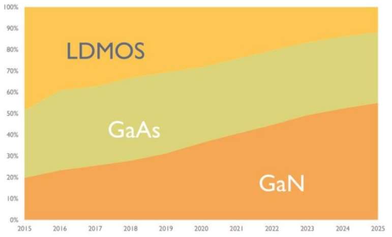
Semi-insulating silicon carbide devices, that is, silicon carbide-based gallium nitride radio frequency devices, are widely used in the field of radio frequency devices. At present, the mainstream RF device materials include different types such as gallium arsenide, silicon-based LDMOS, and silicon carbide-based gallium nitride. Among them, gallium arsenide devices have been widely used in power amplifiers, and silicon-based LDMOS devices have also been used in the communication field for many years, but they are mainly used in low frequency fields less than 4GHz. Silicon carbide-based gallium nitride radio frequency devices have both the high thermal conductivity of silicon carbide and the advantages of high-power radio frequency output of gallium nitride in the high frequency band. With the information technology industry’s demand for data traffic, higher operating frequency and bandwidth Continuously growing, GaN devices are more and more widely used in base stations. Gallium nitride radio frequency devices are replacing LDMOS in communication macro base stations, radar and other broadband applications. According to Yole’s prediction, by 2025, in the RF device market with a power of more than 3W, GaAs device market share will remain basically unchanged, and GaN RF devices are expected to replace most of the silicon-based LDMOS share, occupying the RF device market About 50% share.
With the growth of the global gallium nitride radio frequency device market, the semi-insulating silicon carbide substrate market is expected to continue to grow. Semi-insulating substrates are mainly used in 5G base stations, satellite communications, radar, etc. With the acceleration of 5G construction, especially the promotion of Massive MIMO technology, the market size of silicon carbide-based gallium nitride devices continues to expand. According to YOLE data, the market size of packaged GaN RF devices in 2020 is about 891 million U.S. dollars, of which more than 99% use silicon carbide substrates. By 2026, this part of the market is expected to grow to 2.222 billion U.S. dollars. The compound growth rate is 17%.
At present, the third-generation semiconductors represented by gallium nitride (GaN) and silicon carbide (SiC) have been news recently. Infineon announced that it will acquire GaN systems, a GaN power semiconductor manufacturer, for US$830 million. The two parties have signed a final agreement. Tesla mentioned at the investor day held recently that it plans to significantly reduce the use of silicon carbide transistors in the next-generation vehicle power system, but this news has caused many industry insiders to question it. In fact, the key to hindering the large-scale application of silicon carbide devices is cost. Restricted by silicon carbide crystal growth speed, processing difficulty and defect density, the cost of silicon carbide has remained high. In other words, the cost issue is actually a technical issue. With the advancement of technology, the price of silicon carbide devices is expected to continue to decline in the future, and its industrial applications will develop rapidly. In terms of silicon carbide production capacity, in terms of substrate and epitaxy, the production capacity of domestic companies is mainly 4 inches, transitioning to 6 inches, while 6 inches has been commercialized internationally, and leading companies have started 8 inches layout, and domestic production capacity is still lagging behind. .
In the future, as the penetration rate of silicon carbide devices in new energy vehicles, energy, industry and other fields continues to increase, the market size of silicon carbide devices is expected to continue to increase. According to Yole’s forecast, the market size of spherical conductive silicon carbide power devices is expected to reach US$6.297 billion in 2027, of which automobiles are the largest application market for conductive silicon carbide power devices. Global new energy vehicle head manufacturers are gradually adopting conductive silicon carbide power devices, and a new round of industrial opportunities is about to explode.
Post time: Mar-17-2023