
With the birth of ChatGPT, the potential of pre-training large models to innovate and transform thousands of industries has been fully demonstrated. Some industry leaders even hailed its advent as the “iPhone moment” of artificial intelligence, and predicted that this is “just something greater Start”.
Why does ChatGPT appear so “different”?
Borrowing from the summary of Harvard University professor Venky Narayanamurti, who proposed the Technology Acceptance Theory (TAM), usefulness and ease of use are the two basic prerequisites for the diffusion of an emerging technology. Measured by this standard, the 2016 AlphaGo-Lee Sedol five-game chess battle can be said to have completed the popular science of the “usefulness” of artificial intelligence, and ChatGPT marks another necessary condition for the proliferation of AI technology-ease of use has been achieved. Subtly seeping into the public mind.
Based on this, the outside world has reason to be optimistic and expect that the artificial intelligence industry has indeed stood at a new starting point for the grand blueprint predicted by giants.
Achieved in computing power, trapped in interconnection?
In many “hindsight” interpretations, the GPT family is often associated with the Transformer model launched by Google in 2017.
The Transformer based on the self-attention mechanism, and Google BERT’s “slaughter” performance and amazing generalization ability for various text tasks, can indeed be called GPT as a foundation for pre-technology and engineering methods. Standing on the shoulders of giants, the GPT developer OpenAI team finally made the final leap with more agile efficiency and more powerful execution.
Looking further, Transformer achieves a more efficient use of hardware computing power than traditional deep learning models such as MLP\LSTM.
On this point, Richard Sutton, the deep learning leader and chief scientist of DeepMind in 2019, once said in his article “Bitter Lessons” that the biggest lesson that can be learned from 70 years of AI research is that the general method of using computing is ultimately the most important. Works, and with a big advantage, the ultimate reason is Moore’s Law, or rather its generalization of the continuing exponential decline in cost per unit of computation, most AI research is done with constant computing power available (in this case, exploiting human experience would be the only way to improve performance), however, over a slightly longer than typical research project, the computational power will increase considerably, and in the long run, the only thing that matters is exploiting calculate.
As Sutton foresees, in recent years, AI hardware computing power has achieved rapid development. In addition to the well-known GPU, AI acceleration chips such as Google TPU (the GPT series was trained through TPUv2 in the early days) and Microsoft Catapult often omit advanced control measures such as out-of-order and prefetch in the traditional general-purpose CPU microarchitecture, and can realize volume The core multiplication and addition unit design of the product neural network is optimized, and the parallel computing capability of the SIMD architecture is fully exploited.
The advancement of algorithms, computing power and their combined engineering methods finally laid the foundation for OpenAI to “work hard to make miracles”.
It is fully expected that under the star effect of OpenAI, global technology giants will launch a series of GPT-like pre-training large models in the next one or two years, which is also expected to further accelerate investment in AI computing power clusters in data centers.
However, it is worth noting that although major chip manufacturers are scrambling to launch AI acceleration chips, and the computing power parameters continue to refresh records, the pre-training large model parameters can easily reach tens of billions, hundreds of billions or even trillions, and its training is still far beyond one The range that can be controlled by AI accelerator cards such as two GPUs often requires the interconnection of multiple processors through the network, and even further form HPC computing power clusters to realize pooled scheduling of computing power resources, so as to meet the distribution of AI large models , parallelized training. When evaluating training efficiency, the total training time of a single batch of data (batch) is often significantly affected by the communication time.
For this reason, with the emergence of a new imaginary space revealed by the AI large model, the infrastructure of computing power clusters will also usher in an investment boom. In a series of engineering challenges such as power distribution, heat dissipation, and communications, computing power Data transmission between nodes is especially the key “bottleneck” that restricts the full release of hardware computing power.
Breaking the “key fulcrum” of interconnection bottlenecks
The exponential growth of the amount of data faced by AI training and reasoning makes data transmission generally present the technical requirements of high bandwidth and low latency, regardless of whether there are multiple GPUs in a single server, C2C communication between CPUs, or networking between multiple servers.
In the context of the convergence of the computing power cluster communication network topology, the switch interface has increasingly become an important breakthrough to break through the “bottleneck”, and derived various engineering ideas such as increasing the speed of the network card, increasing the number of network cards, and even applying RDMA network direct connection.
In the field of low-level interface technology, compared with traditional parallel interfaces, SerDes serial interfaces have become the mainstream of applications due to their significant cost advantages. In new standards such as PCIe 6.0, PAM4 (fourth-order Pulse Amplitude Modulation) encoding is supported to further increase the SerDes data transfer rate.
However, the application of SerDes naturally has many technical challenges, the most serious of which is undoubtedly the problem of signal integrity (SI).
For example, in mid-distance and long-distance interconnection scenarios through backplanes, connectors, and PCB boards, the TX and RX ends of SerDes high-speed links are often separated by pins, PCB vias, signal lines, and even connectors, cables, etc. , there are noise, crosstalk, and signal attenuation introduced by complex reasons such as materials, processes, and layouts, so that the electrical signal that finally reaches the receiver may be severely distorted, and it is difficult to recover the clock and data bits of the transmitted information, which also limits the speed and distance. on the design space.
The new generation of 56G and 112G SerDes uses PAM4 encoding. While providing greater network throughput, it also introduces more levels, resulting in loss of signal-to-noise ratio, deterioration of bit error rate (BER), forward error correction ( FEC) issues such as increased latency require careful trade-offs.
From the above analysis, it is not difficult to see that in order to give full play to the computing power of AI hardware, interface technology is the key fulcrum to break the bottleneck of interconnection, which has a great leverage effect, and its application must solve many challenges surrounding signal integrity.
At present, although a large number of hardware manufacturers have hired full-time SI engineers to be responsible for debugging, the effect depends on various personal “skills”. Since signal integrity needs to be guaranteed at all levels of chip and system design, the verification process is often protracted. Only a skilled and experienced design team in the field of analog electronics can try this kind of design, and the test verification cycle is long.
Because of this, in chip design, outsourcing high-speed interface IP has almost become a “must” in the industry, and it has also driven interface IP to become the fastest growing IP market segment in recent years. Before and after surpassing CPU IP, it became the largest semiconductor IP category.
Teach a man to fish, teach a man to fish
The interface IP market opportunity also makes it a hot spot of competition among major IP HOUSEs. For example, Cadence, one of the world’s three major IP manufacturers, also launched its 112G SerDes IP design, which is oriented to the SOC requirements of high-performance computing (HPC) data centers, suitable for long-distance and medium-distance transmission, and has passed the 7nm process Silicon-proven, with excellent PPA performance, insertion loss >35dB.
It is worth mentioning that the outsourced interface IP is only the starting point from chip to system development and signal integrity testing. Whether the tools supporting the workflow are complete and accessible is also an important factor affecting the development cycle. It is not only to teach a man to fish, but also to teach a man to fish.
As a giant in the EDA\IP field, Cadence’s practice in this area is particularly representative. In addition to mature interface IP such as SerDes, the company also provides comprehensive design tools and technologies that are organically integrated to help chip and system designers deal with signal integrity challenges at all levels.
For example, in the interconnection design and simulation between different chips, modeling is an essential means. Currently, IBIS and AMI are the preferred methods for modeling SerDes channels. The emergence of IBIS-AMI makes it possible to quickly and accurately simulate a large number of bit streams using simulation models. As one of the definers of industry standards, Cadence is also at the forefront in the development of related tools. Based on its Sigrity Advanced IBIS modeling tool, users can automatically create models and generate practical algorithm models with the help of wizard programs.
In medium and long-distance interconnection scenarios based on PCB boards/backplanes/connectors, developers of SerDes high-speed interfaces need to perform signal integrity (SI) and power integrity (PI) for the overall design in order to analyze signals accurately and reliably. As well as electromagnetic compatibility (EMC) co-simulation, developers often need to have a thorough understanding of data acquisition and analysis theory, and accurately establish analog device characteristic models.
In response to this pain point, Cadence’s Solver provides a better tool selection for PCB, IC packaging and SoIC key interconnect design. Based on the high-precision S-parameter model created by it, even at 112G data transmission speed, it can also achieve the same The laboratory measurements matched the simulation results. Its finite element analysis (FEM) process achieves a high degree of parallelization, which can greatly reduce the time spent on solving, and supports nearly linear scalability of hardware computing power.
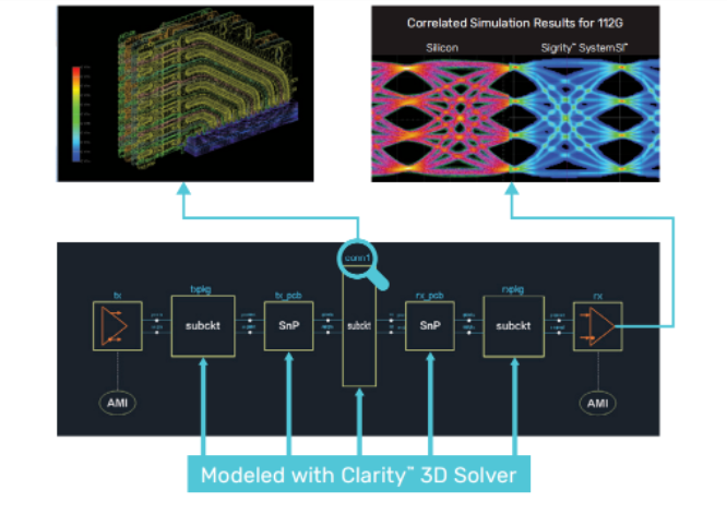
Also, when analyzing link signal integrity, there is often an implicit assumption that the board and connector are functioning well, but at very high frequencies, the assumption that the connector and board are analyzed separately and then “connected” together No longer applicable. The excessive interaction between boards and connectors also requires comprehensive 3D analysis tools such as Clarity Solver to achieve high-quality designs while accurately predicting finished product performance.
After Huang Renxun called out the “iPhone moment” of artificial intelligence, in just a few dozen days, the pre-training large model and its downstream applications have shown a dizzying explosive trend. It is conceivable that in the “arms race” of AI large-scale models of major cloud computing giants, computing power clusters will also usher in a new round of investment boom, and communication network and interface technologies are also expected to enter a period of accelerated development. In addition, Tesla Dojo, Cerebras WSE-2 and other manufacturers who take the “super single chip” route may also lead a new way of large-scale model training.
However, no matter what the path is, the “rigid demand” for interface IP is clearly visible. In this hot and difficult field, the author also expects more major manufacturers such as Cadence to bring complete solutions to promote the alleviation and loosening of interconnection bottlenecks. , effectively release the infinite possibilities of pre-trained large models, and benefit thousands of industries.
Post time: Apr-22-2023