
Wafer bonding is an emerging semiconductor processing technology that has developed rapidly in the past ten years. It has important applications in the fields of MEMS, CIS and memory chips, and has received more and more attention.
In the ocean of information, the existence of wafer bonding is extremely thin compared to lithography technology, but when we take out a mobile phone, its image sensor, gravity acceleration sensor, microphone, 4G and 5G RF front-end, and some NAND is more or less applied to wafer bonding technology. It can be said that wafer bonding technology has made an important contribution to our information life.
Wafer bonding can be distinguished from wire bonding and die bonding applied in traditional packaging by its name. In Japanese, bonding is translated as joining, which makes it easier to understand the craft and process from the intuitive impression.
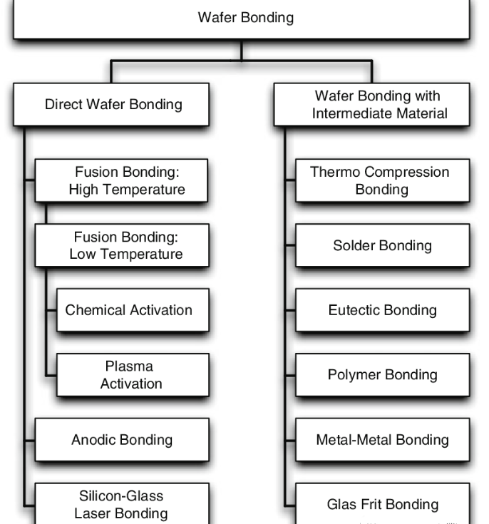
In terms of bonding methods, wafer bonding can be divided into permanent bonding and temporary bonding. The difference is also as the name implies, there is no need to debond after permanent bonding, while temporary bonding requires debonding to reopen the bonded wafers.
In terms of interface materials, it is divided into adhesive bonding with an intermediate layer, eutectic bonding, metal thermocompression bonding, fusion bonding without an intermediate layer, and anodic bonding.
Source: Wafer Bonding, Shawn Cunningham & Mario Kupnik, Chap.11
The purpose of bonding is also different, such as providing airtight protection for devices, certain application scenarios in MEMS and SAW; another example is to provide mechanical support or layer transfer for thinning wafers, such as applications in IGBT and BSI Based on this purpose; the latest and most important application is the three-dimensional interconnection of transistors, HBM, 3D NAND, complementary field effect transistor CFET and back power supply network BPN under development, etc., hybrid bonding (hybrid bonding) that has emerged in recent years It is the process that focuses on this application, which is named because it includes both fusion bonding and metal bonding characteristics.
Early wafer bonding did not have high requirements for overlay precision control, which can be within 10 microns after bonding. However, since the start of BSI, the overlay accuracy requirement has reached the level of 1.5 microns, and for the application of 3D NAND and high-end BSI, it has reached the requirement of less than 300 nanometers or even 150 nanometers! With the development of bonding technology and the penetration of front-end technology, the author boldly speculates that the requirement for overlay accuracy of tens of nanometers may be reached in the future.
Old wine in new bottle
As mentioned earlier, the essence of bonding is bonding, and the principle of using various physical and chemical methods to bond two interfaces has been discovered and applied long before humans cut out the first wafer. Whether it is glue bonding with the help of polymer compounds, eutectic bonding using the welding principle, or even fusion bonding through the van der Waals force between ultra-smooth surfaces, the basic principle has been established before the birth of wafer bonding. It has long been known. However, the real large-scale industrial application of wafer bonding has only begun in the last ten years.
In 1969, Wallis and Pomerantz first described the use of an electric field at 500°C to bond silicon wafers and soda glass wafers together, what we know today as anodic bonding.
In 1986, IBM and Toshiba discovered fusion bonding in their research. When a silicon wafer is mirror-polished, it can bond with each other through van der Waals force even at room temperature without the help of other bonding media. This is also silicon-silicon. The beginnings of direct bonding. In the following years, fusion bonding techniques for SOI, MEMS, and III-V compounds were published. After the 1990s, room temperature bonding + low temperature annealing using plasma treatment of the wafer surface and fusion bonding technology without annealing under high vacuum have also been developed one after another.
In 2016, Sony produced image sensors using copper-silicon dioxide hybrid bonding for the first time. This idea, which began in the mid-1980s, has finally become a reality after more than ten years of research and has been accepted by the industry.
Source: Handbook of Wafer Bonding, Chap.15
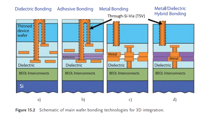
There are many ways to achieve three-dimensional interconnection through wafer bonding, but the fusion bonding scheme shown in (a) and the hybrid bonding scheme shown in (d) are more suitable for advanced CMOS processes.
Metal thermocompression bonding (c) requires extremely high pressure (10-100kN), and even similar to anodic bonding, it also uses a high-voltage electric field. It is not so friendly to CMOS process compatibility, and it is easy to damage the metal in front of it. Graphics, so fusion bonding and hybrid bonding (d) that only require room temperature bonding + low temperature annealing are gaining more and more favor because of their good process compatibility with CMOS.
Fusion bonding is not inherently so mild. From the early process conditions that require high temperature annealing at 1000°C for several hours, it has developed to only require normal pressure plasma surface activation and bonding at room temperature, and annealing at less than 400°C. There is no need for annealing after plasma surface activation under ultra-high vacuum, which provides a guarantee for its strong CMOS process compatibility. The hybrid bonding that directly uses copper contacts for interconnection without the help of TSV shortens the interconnection distance between the upper and lower wafers to the shortest and further improves the electrical performance.
It is precisely because of the rapid development of fusion bonding and hybrid bonding that the biggest obstacle for wafer bonding to CMOS interconnection technology has been removed.
Fusion Bonding: From SOI to BSI
Fusion bonding usually uses silicon-silicon or silicon-silicon dioxide as the bonding interface, and is bonded after appropriate surface treatment. The author has seen a saying that as long as the surface is smooth and flat enough, everything can be bonded, so special substrates such as indium phosphide and lithium niobate can also be fusion bonded to silicon wafers!
An early relatively well-known application of fusion bonding was for the production of silicon-on-insulator in SOI. As a substrate material with rich optical and electrical properties, the preparation of SOI is naturally more complicated than conventional silicon wafers. Bare silicon wafers and thermal oxygen wafers are thinned on the back side after fusion bonding, which is the main preparation method of early SOI wafers. However, due to its high cost, slow production speed, and poor uniformity, its application scenarios are relatively restricted. Afterwards, the SmartCut® technology developed by Soitec in France has greatly improved the cost, production speed and uniformity index. After the bare silicon wafer is used as the donor wafer, after fusion bonding, the hydrogen ion implantation will automatically break and separate the donor. Wafers, which are reusable after surface polishing.
A more well-known application of fusion bonding is the production of BSI back-illuminated image sensors. In the initial stage of BSI, after the non-patterned wafer as a mechanical support and the CMOS wafer were melt-bonded, the back of the CMOS was thinned for the fabrication of the pixel array. With the development of the demand for image signal processing, face-to-face fusion bonding of image processing logic wafers and CMOS wafers, and interconnection with TSVs has become a new manufacturing method. When the hybrid bonding technology matures, BSI has also entered the era of high-density interconnection, which is a later story.
In addition, the author has also seen cases in some papers where fusion bonding is used to interconnect chips such as micro LEDs and MEMS with CMOS. In the CFET technology route including IMEC, there is also the application of using fusion bonding to make three-dimensional transistors. With the advent of the three-dimensional era of semiconductors, the potential of fusion bonding is immeasurable.
Hybrid Bonding: A Business Card for a New Era
When it comes to the most typical application of hybrid bonding, there is no doubt that it is YMTC’s Xtacking®. Through different processes, memory wafers and CMOS wafers are produced successively, and the contacts between the two are built in the subsequent process. Through hybrid bonding, these contacts are connected by links, and Memory and CMOS are interconnected in the vertical direction.
According to the Frauebhofer Institute, the advantages of hybrid bonding are threefold:
Shorter interconnection distance: not only do not need to use leads to communicate with each other, but also do not need to use TSV to pass through the entire CMOS layer, and the interconnection can be realized only by connecting the copper contacts in the back channel
Higher interconnect density: the area of copper contacts is very small. Compared with solder balls and TSVs with a diameter of 100 microns, the pitch size of copper contacts in the hybrid bonding process is even less than 10 microns, which undoubtedly can achieve higher interconnection density
Lower cost: There is no doubt that it takes more time to interconnect each DIE individually. Large-area and high-density interconnections can be achieved through wafer bonding, and the contribution to the increase in production capacity is leaps and bounds! Naturally, production costs can also be reduced
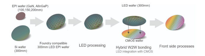
In addition to the previously mentioned BSI, cases such as micro LED and CMOS for hybrid bonding also exist. In the latest research, there is even a practice of cutting micro LEDs into independent DIEs and bonding them to a 12-inch wafer after they are fabricated on a small-sized wafer, and then performing hybrid bonding and interconnection with a CMOS 12-inch wafer. , it can be seen that its process compatibility is very good. This is another advantage of hybrid bonding. CMOS of different technology nodes can also be interconnected through copper contacts, and the flexibility of process selection has also been greatly improved!
Of course, hybrid bonding is not perfect. For example, it is impossible to know the failed DIE from the initial stage. It can only be distinguished after the integration, thinning and dicing and passing the test. Therefore, the yield of the finished DIE will be greatly affected. Secondly, the bonding interface requires ultra-high flatness, and the internal stress of the wafer also needs to be controlled to reduce wafer warpage, all of which put forward strict requirements for the control of the subsequent process. Compared with traditional packaging technology, the cleanliness level above ISO3 required for hybrid bonding is much higher than the cleanliness requirements of ISO5 in traditional packaging and testing plants, which puts forward high requirements for factory affairs and environmental management and control.
Top player
The realization of the technology needs to rely on the support of materials and equipment. Although it is a post-processing technology, there are very few players in it. Among them, Karl Suss from Germany and EVG (EV Group) from Austria take the lead. Japan Although Canon and Mitsubishi of China also have special types of bonding equipment, neither the market share nor the technical level can be compared with these two top players. At present, the only document in China that systematically introduces wafer bonding is the “Wafer Bonding Handbook”, in which the equipment of Seuss and EVG has a high rate of exposure and has been mentioned repeatedly. Its popularity and leading position are self-evident.
The product lines of Seuss and EVG have a high degree of overlap, and both sides cover almost all types of bonding processes at the same time. In addition to bonding machines, they also include alignment machines and double-sided photolithography machines for wafer alignment, and Measuring machines for testing bonding accuracy are also available, but each has its own merits. In the domestic bonding machine market, compared with EVG, Suss has a better reputation and market share in universities and research institutes, but EVG is even better in industrial applications. Especially the domestic advanced BSI production line, EVG’s fully automatic fusion bonding machine GeminiFB has almost reached 100% market share!
At present, domestic bonding machines are still mainly low-end. Although the bonding machines developed and produced by Shanghai S Company have penetrated the market of adhesive bonding and metal bonding, they have not yet entered the main position of fusion bonding. Another domestic company that focuses on bonding machines is H Company. Like S Company, H Company is a company known for its lithography subsystem. Its 200nm alignment accuracy is still not comparable to that of EVG’s previous generation products, but It is also a major breakthrough for local enterprises! In addition, several semiconductor equipment manufacturing companies are developing new bonding equipment. After all, until last year, the growth of the CIS industry has continued for 10 years, and the market space is quite broad! Although the CIS market will experience its first decline in 10 years in 2022, with the increasing demand for security and smart cities, the CIS market is large enough to accommodate players other than SUS and EVG.
At the end
In the past ten years, the pace of advancing Moore’s Law has gradually slowed down. More and more semiconductor companies are seeking advanced packaging to drive the improvement of chip performance. Heterogeneous integration is one of the solutions, and the wafer bonding process provides it with high efficiency. The realization path becomes a strong candidate process!
When Intel and IMEC announce the future development route of transistors in 2022, and enter the CFET era after 1nm, I firmly believe that fusion bonding and hybrid bonding will move from the back to the front, together with high NA and hyper NA EUV lithography machines Lead the development of the semiconductor industry for the next 15 years!
Post time: May-04-2023