
Last week, Google published its in-depth interpretation of TPU v4 paper “TPU v4: An Optically Reconfigurable Supercomputer for Machine Learning with Hardware Support for Embeddings” on the paper preprint platform arxiv (TPU v4: reconfigurable machines through optical interconnection) Learning supercomputer, equipped with hardware embedding layer acceleration). The paper will be officially published at ISCA 2023 (International Symposium on Computer Architecture, the top conference in the field of computer architecture) in June this year, and the current preprint undoubtedly provides us with the opportunity to get a glimpse of its whole picture.
As can be seen from the title of the paper, one of the main highlights of Google TPU v4 is reconfigurability and high scalability through optical interconnection (that is, “optically reconfigurable” in the title). At the beginning of the thesis, what Google first introduced was not the traditional MAC design, on-chip memory, HBM channel and other common parameters of AI chips, but the configurable optical interconnection switch (reconfigurable optical switch). As the top priority of the paper, here we also analyze in detail why optical interconnection occupies such an important position in the design of TPU v4, so that Google even developed an optical chip for it.
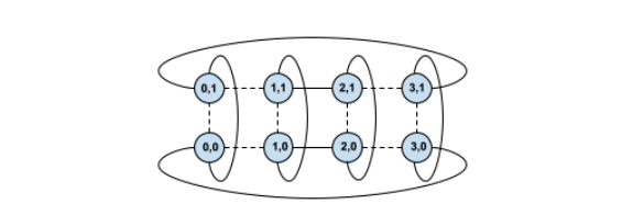
When TPU v4 was designed from the beginning, its goal was extremely high scalability, and thousands of chips can be accelerated at the same time, so as to realize a supercomputer designed for machine learning model training. In Google’s design, the topology of the supercomputer is: 4x4x4 (64) TPU v4 chips are interconnected to form a cube structure (cube), and then 4x4x4 such cubes are connected together to form a total of 4096 TPU v4 supercomputer.
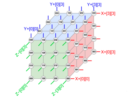
In such a topology, TPU v4s that are physically close (that is, chips in the same 4x4x4 cube) can be connected by conventional electrical interconnection (such as copper wires), but TPUs that are far away (such as in The interconnection between cubes) must use optical interconnection, the reason is that in such a large-scale supercomputer, the data interconnection between chips will largely determine the efficiency of the overall calculation; if the data interconnection efficiency is not high enough , many times the chip is waiting for data from other chips to arrive to start computing, thus creating a waste of efficiency. In order to avoid such a situation of “chips and other data”, it is necessary to ensure that the interconnection between chips can have high bandwidth and low latency. Optical interconnection has become the first choice for chips with long physical distances.
The use of optical interconnects in high-performance computing is not new, and Google’s main breakthrough in TPU v4 is to use reconfigurable optical interconnects (that is, add optical circuit switches, optical circuit switch OCS) to quickly realize different chip interconnections topology. In other words, the interconnection between chips is not static, but reconfigurable in the field. Doing so has many benefits, chief among them being the ability to change topology based on specific machine learning models and improving the reliability of supercomputers.
In terms of topology, the requirements of different machine learning models for data flow can be roughly divided into three categories, namely, data parallelism (each chip loads the entire model, and different chips process different data in the data set), model parallelism (model Some layers in the model are very large, so each chip is only responsible for a part of the calculation of such a large layer), and pipeline parallelism (different layers in the model are handed over to different chips for calculation), and different data streams correspond to different TPU interconnection topology. When there is a reconfigurable optical interconnection, the interconnection topology between TPUs can be adjusted according to the specific model data flow, so as to achieve optimal performance, which can be improved by more than 2 times.
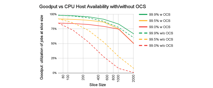
Another advantage is reliability. In such a supercomputer composed of a large number of chips, an important consideration is how to ensure that the overall supercomputer can still maintain high performance if a small part of the chips fail to work? With conventional fixed interconnect architectures, a single chip failure could affect the entire system. With a reconfigurable optical interconnect, all that needs to be done is to bypass the faulty chip, which will not affect the work of the entire system, and will sacrifice a little overall performance at most. In the paper, Google gave a graph of the single-chip failure rate and the average performance impact of the system. When using configurable optical interconnects (and optical path switches), assuming that the chip reliability rate is 99%, the overall system The average performance improvement ratio does not make OCS can be as high as 6 times, the importance of visible light interconnection switches.
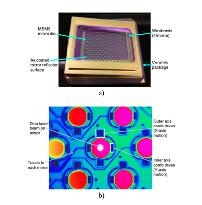
In order to realize configurable optical interconnection at the data center level, it is necessary for the optical switch to efficiently expand to a very high number of interconnections (such as 1000×1000), and at the same time it is necessary to achieve low switching delay, low cost, and low signal loss. Google believes that the existing commercial solutions are not satisfactory enough, so Google developed an optical switch chip Palomar, and used this chip to realize the world’s first data center-level configurable optical interconnection, and TPU v4 is the matching This self-developed optical switch chip achieves high performance from the architecture. Google’s self-developed optical path switch chip Palomar uses technology based on MEMS mirror arrays. The specific principle is to use a 2D MEMS mirror array to adjust the optical path by controlling the position of the mirrors, thereby realizing the switching of the optical path. Optical switch chips using MEMS can achieve low loss, low switching delay (millisecond level) and low power consumption. After a series of optimizations, the cost of the optical path system is also kept low, accounting for less than 5% of the cost of the entire TPU v4 supercomputer.
Algorithm-chip co-design is the soul of TPU v4
If reconfigurable optical interconnection provides a good foundation for TPU v4, then algorithm-chip collaborative design is the soul of TPU v4. Algorithm-chip collaborative design includes two parts, one is how to optimize the chip according to the algorithm, and the other is how to optimize the algorithm according to the chip. In the TPU v4 architecture, both of them have been carefully considered.
We first analyze how TPU v4 optimizes the chip according to the algorithm. If it is said that when TPU v1 was released in 2017, it mainly solved the convolutional neural network CNN, then in 2023, the acceleration problem of CNN has already been considered to be almost the same, and more is how to deal with the current booming large model The problem. For Google, the most critical large model at present is the large model of the recommendation system that determines the company’s main revenue. Therefore, the design of TPU v4 is also quite optimized for the large model of the recommendation system. In large models of recommender systems, the current acceleration bottleneck is the embedding layer. The purpose of the embedding layer is to map high-dimensional sparse features to low-dimensional high-density features, so that the high-density low-dimensional features can be further processed by the neural network. The implementation of the embedding layer is usually a look-up table (look-up table), and this look-up table can be very large to the order of 100GB. There can be multiple such lookup tables in a recommendation system model, so that the storage capacity of the entire lookup table can reach TB level. Such a huge lookup table will require the use of distributed computing, and the lookup table of each embedded layer will be distributed to multiple TPU v4 chips for calculation. Google mentioned in the paper that when performing such embedding layer calculations, the calculations are mainly based on 1D vector calculations, rather than 2D matrix or 3D tensor calculations; secondly, calculations are often sparse (because the input features are sparse, Therefore, not all features will have high-density calculations) and are distributed on different chips, so it is necessary to optimize shared storage so that different chips can exchange data efficiently.
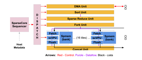
In order to optimize the embedding layer, Google specially designed a dedicated acceleration module in TPU v4, called SparseCore (SC). Each SC has its own vector computing unit (scVPU), 2.5 MB local SRAM, and a memory access interface that can access up to 128TB shared HBM. In addition, SC also has some dedicated acceleration logic specially designed for embedded layer operations, including sorting (Sort), statute (Reduce), splicing (Concat), etc. We can see that the structure of each SC is actually relatively simple, so a large number of SCs are deployed in each TPU v4, but at the same time, the overall area and power consumption of SCs account for about 5% of TPU v4. In the paper, Google compared using the CPU to run the embedding layer (which is also the way to run the embedding layer routinely) and using the TPU v4 SC to run the embedding layer. The results show that when running the same recommendation system, compared to running the embedding layer on the CPU, Putting the embedding layer on the SC of TPU v4 can increase the running speed of the overall recommendation system by more than 6 times. In fact, this is also the most attractive part of domain-specific design, that is, a very large performance improvement can be obtained with a small chip area and power consumption overhead. In the design of TPU v4, Google puts such a domain-specific design in the most critical place for the entire company (the core bottleneck embedding layer of the recommendation system model that determines Google’s overall revenue), thereby leveraging very large benefits.
In addition to optimizing algorithms at the chip level, TPU v4 also optimizes algorithms at the distributed computing topology level. As we mentioned in the previous article, the introduction of reconfigurable optical interconnection in TPU v4 can realize the interconnection topology between different TPU v4 for different artificial intelligence models. For this reason, Google designed a set of machine learning algorithms to determine how to Model to configure optical path switches to improve performance. The analysis shows that for the training of the most popular large language models (including GPT-3), the optimal TPU optical interconnect topology configuration found by machine learning algorithms can improve the performance by 1.2-2.3 times.
Finally, Google also specially designed a neural network architecture search (NAS) algorithm for TPU v4, which can optimize the artificial intelligence model according to the characteristics of TPU v4, so as to ensure that the optimized model can run on TPU v4 most efficiently, and Make full use of the resources of TPU v4. Compared with manual optimization, the use of this NAS can achieve up to 10% runtime optimization of the recommendation system, which is roughly equivalent to saving tens of millions of dollars in annual costs.
TPU v4 and the future of artificial intelligence chips
From the design of TPU v4, we can see some future directions of artificial intelligence chips, and these directions are what we have also seen in the design of other mainstream artificial intelligence chips such as Nvidia’s GPU:
The first is support for efficient interconnection and scale. As artificial intelligence models become larger and larger, the support for such models mainly depends on the scalability of artificial intelligence chips (that is, how to enable multiple chips to efficiently and reliably work together to accelerate such large models), rather than blindly Improve the ability of a single chip to support large models, because the evolution of the model is always faster than the design iteration of the chip. In this field, different chip companies will have different emphases. For example, AMD focuses on using chiplets at a more microscopic level to achieve scalability at the packaging level. Nvidia has chip technologies such as NvLink to achieve scalability and compatibility between multiple cards in a single machine. Performance improvement, Google directly designed an optical switch chip for mass TPU interconnection; but the commonality between these companies, that is, the support for the scalability of artificial intelligence chips to meet the needs of large models, is quite consistent. From this point of view, future scalability (such as data interconnection bandwidth) may become the main index of artificial intelligence chips as well as peak computing power, and this also makes artificial intelligence chip design more cross-border: that is, it is not only necessary for Resources in digital logic and computer architecture also need to be accumulated in the fields of packaging and data interconnection.
In addition, the combination between artificial intelligence chips and algorithms continues to maintain a close relationship, and algorithm-chip collaborative design will still be one of the main means for future artificial intelligence chips to continue to improve performance. We have seen a lot of achievements of Google, Nvidia, etc. in algorithm-chip co-design: including support for new number systems (Nvidia’s FP16, FP8, Google’s BF16, etc.), support for computing features (Nvidia for sparse computing support), and the deployment of direct dedicated accelerators for key algorithms of the model (Nvidia’s transformer accelerator, Google’s SC, etc.). As Moore’s Law is getting closer and closer to the physical limit in the future, it is expected that the further improvement of the performance of artificial intelligence chips in the future will rely more and more on algorithm-chip collaborative design. The performance of artificial intelligence will still maintain a near-exponential improvement similar to Moore’s Law, so artificial intelligence chips will still be one of the most popular directions in the semiconductor industry in the next few years, and will also become an important engine for the continued development of the semiconductor industry in the future.
Post time: Apr-10-2023