
You can make a lot of things with silicon photonics, but lasers aren’t one of them.
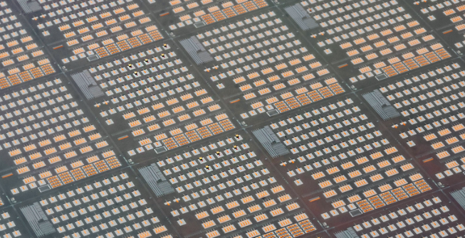
Photonic integrated circuits, which combine a range of optoelectronic functions on a single chip, are becoming more and more common in everyday life. They’re used in high-speed optical transceivers that connect server racks in data centers, including those used to transmit IEEE Spectrum websites, lidar used to keep self-driving cars on track, and used to spot chemicals in the atmosphere spectrometers, and many other applications. All of these systems have become cheaper and, in some cases, have become economically viable by using silicon fabrication techniques to make most of the integrated circuits.
Engineers have been able to integrate nearly all important optical functions on silicon photonic chips, including the basic functions of modulation and detection, except for one: light emission. Silicon cannot do this efficiently by itself, so semiconductors made of so-called III-V materials, named for their composition’s position on the periodic table, are often used to make individually packaged components to emit light.
If you can use an external laser diode in your design, no problem. But several factors have recently prompted engineers to integrate lasers with silicon photonics. For example, there may not be room for a separate light source. Tiny devices implanted in the body to monitor blood sugar levels may face this problem. Or the cost of the application might require tighter integration: when you can fit hundreds or thousands of lasers on a single silicon chip, you end up with lower cost and higher reliability than if you had to connect separate chips.
There are many ways to achieve this tighter integration of lasers and silicon. Working at Imec, the nanoelectronics R&D center in Belgium, we are currently pursuing four basic strategies: flip chip processing, micro transfer printing, wafer bonding and monolithic integration. Below is a guide on how these approaches work, their scalability and maturity levels, and their pros and cons.
Flip Chip Integration
A straightforward method of integrating lasers directly onto silicon wafers is chip packaging technology, known as the flip-chip process, as the name suggests.
The chip’s electrical connections are on top, with the uppermost interconnects terminating in metal pads. Flip-chip technology relies on solder balls attached to these pads. Then flip the chip over so the solder lines up with the corresponding pads on the chip’s package (or in our case the other chip). The solder then melts, bonding the chip to the package.
The concept is similar, but more rigorous, when trying to bond laser chips to silicon photonic chips. Edge-emitting lasers are fully processed on the wafer, diced into individual chips, and tested by suppliers. The individual laser chips are then bonded to the target silicon photonics wafer, one laser chip at a time, using a high-precision version of the flip-chip process. The hard part is making sure the output of the edge-emitting laser aligns with the input of the silicon photonic chip. We use a process called butt-coupling, where the laser is placed in a recessed part of the silicon so it laterally adjoins the etched facet of the silicon photonic waveguide.
To do this, the flip-chip process requires sub-micron alignment accuracy in all three dimensions. Over the past few years, specialized flip-chip bonding tools have been developed to do this job, and we and our collaborators and development partners have used them to optimize the assembly process. With advanced pick and place tools that use machine vision to maintain precise alignment, we can place and bond laser devices with better than 500 nanometer precision in just tens of seconds.
In 2021, we also built a wafer-level silicon photonics process to improve this performance. It adds mechanically aligned pedestals and more precisely etched butt-coupling interfaces to silicon chips to achieve vertical alignment better than a few hundred nanometers. Using these techniques, we assembled certain laser devices on 300mm silicon photonics wafers. We were delighted to see that as much as 80 percent of the 50 milliwatts of laser light from each device is coupled into the silicon photonics chip it is connected to. In the worst case, the coupling is still around 60% across the wafer. These results are comparable to the coupling efficiencies achieved by active alignment, a more time-consuming process in which light from the laser itself is used to guide the alignment process.
A significant advantage of the flip chip approach is the simplicity and flexibility of paired chip types. Because they can be produced on existing production lines with limited additional engineering, they can each be sourced from multiple manufacturers. Moreover, as the market demand increases, more and more suppliers provide flip chip assembly services. On the other hand, the sequential nature of the process — each laser chip needs to be picked and placed individually — is a significant drawback. In the long run, it limits manufacturing throughput and the potential for substantial cost reductions. This is especially important for cost-sensitive applications such as consumer products and systems requiring multiple laser devices per chip.
Microtransfer
Microtransfer printing removes some of the alignment difficulties of butt couplings, while also speeding up the assembly process. Like the flip-chip process, light-emitting devices are grown on III-V semiconductor substrates. But there is one big difference: III-V wafers are not diced into individual chips. Instead, the lasers on the wafer are undercut so they are only connected to the source wafer by a small tether. The devices are then picked up together with an ink stamp-like tool to break the tether. The stamp then aligns the lasers with the waveguide structures on the silicon photonics wafer and bonds them there.
Flip-chip technology uses metal solder bumps, while microtransfer printing uses adhesives, and it can even be done with molecular bonding alone, which relies on van der Waals forces between two planes, held in place by a laser. Furthermore, the optical coupling between light sources and waveguides in silicon photonic chips occurs through different processes. The process, called evanescent coupling, places the laser on top of the silicon waveguide structure, into which the light then “bleeds.” Although less power is transferred in this way, evanescent coupling requires less alignment accuracy than butt coupling.
Having greater alignment tolerances enables this technology to transfer thousands of devices at a time. Therefore, in principle it should allow higher throughput than flip-chip processing and is ideal for applications requiring the integration of a large number of III-V components per unit area.
While transfer printing is an established process for making microLED displays, such as those required for many augmented and virtual reality products, it is not ready to print laser or optical amplifiers. But we got there.
Last year, Imec successfully used transfer printing to attach such light sources to wafers containing silicon photonic waveguides, high-speed light modulators and photodetectors. We have also printed infrared lasers tunable beyond 45 nm wavelengths and high pulse energy devices for chip-based spectroscopy systems. These were made just for demonstration purposes, but we don’t see the root cause of this approach not being able to achieve good results with high yields. Therefore, we expect the technology to be ready to be deployed on production lines within a few years.
![In flip-chip bonding, laser chips [left] are individually transferred and bonded to silicon photonics wafers.](https://www.vihochips.com/uploads/In-flip-chip-bonding-laser-chips-left-are-individually-transferred-and-bonded-to-silicon-photonics-wafers..png)
Precise alignment of light-emitting elements with their silicon photonics partners is a critical step for both technologies we discuss. But one technology, one called III-V silicon wafer bonding, has found a way around it. Instead of transferring the built laser (or other light-emitting component) to a processed silicon wafer, the solution is to bond a blank chip (or even a small die) of a III-V semiconductor to the silicon wafer. You can then build the desired laser device where the corresponding silicon waveguide already exists.Among the transferred materials, we are only interested in thin layers of crystalline III-V matrial, called epitaxial layers. Therefore, after bonding to the silicon wafer, the rest of the material will be removed. Laser diodes can be fabricated in epitaxial layers aligned with underlying silicon waveguides using standard photolithography and wafer-level processes. Any unwanted III-V material is then etched away.
Engineers at Intel have developed the approach over the past decade, and in 2016 introduced the first commercial product built with it—an optical transceiver. This approach allows for high-throughput integration as it can process many devices in parallel at the same time. Like transfer printing, it uses evanescent coupling between III-V and silicon materials, resulting in a highly efficient optical interface.
One downside of III-V bonding to silicon wafers is that you need a significant investment to set up a production line that can handle the III-V process steps using the tools used to make silicon wafers in 200 mm or 300 mm diameter. This tooling is very different from the tools used in laser diode foundries, where typical wafer diameters are much smaller.
![In die-to-wafer bonding, blank wafers of III-V semiconductors [pink] are bonded to already processed silicon photonics wafers. III-V materials are processed into lasers over silicon waveguides. The rest of the II](https://www.vihochips.com/uploads/In-die-to-wafer-bonding-blank-wafers-of-III-V-semiconductors-pink-are-bonded-to-already-processed-silicon-photonics-wafers.-III-V-materials-are-processed-into-lasers-over-silicon-waveguides.-The-rest-of-the-II.png)
The ideal way to combine the two different materials involved would be to grow the III-V semiconductor directly on silicon, an approach known as monolithic integration. This will eliminate any need for gluing or alignment, and will reduce the amount of wasted III-V material. But to make this strategy practical, many technical hurdles must be overcome. As a result, research at Imec and elsewhere continues toward this goal.
The main goal of the research was to create crystalline III-V materials with low defect densities. The fundamental problem is that there is a considerable mismatch between the lattice spacing of the atoms in silicon and the lattice spacing of the atoms in the III-V semiconductors of interest—more than 4 percent.
Because of this lattice mismatch, every III-V layer grown on silicon is strained. After adding just a few nanometers of III-V film, defects appear in the crystal, releasing the built-up strain. These “mismatch” defects form along lines that penetrate the entire III-V layer. These defects include open crystal bond lines and localized crystal distortions, both of which can severely degrade the performance of optoelectronic devices.
To prevent these defects from destroying the laser, they must be confined away from the device. Doing so typically involves laying down a layer of III-V material a few microns thick, creating a large buffer zone between the mismatch defect below and the strain-free region above, where the laser device can fabricate it. Researchers at the University of California, Santa Barbara report excellent progress using this approach, demonstrating highly efficient gallium arsenide-based quantum dot lasers with reliable lifetimes.
However, these experiments have only been performed on a small scale. Scaling the technology to the 200 or 300mm wafers used in industry will be difficult. Adding a thick buffer layer can cause various mechanical issues such as cracks inside III-V films or wafer bowing. Also, since the active devices sit on top of such a thick buffer layer, it is difficult to couple light into the underlying waveguides in the silicon substrate.
To circumvent these challenges, Imec has introduced a new method of monolithic integration called nano-ridge engineering, or NRE. The technique aims to force defects to form in such a confined space that working devices can be built a little more than 100 nm above the interface with the underlying silicon.
NRE uses a phenomenon called aspect ratio trapping to confine defects to small areas. It begins by forming narrow and deep trenches in a silicon dioxide insulator layer. At the bottom of the trench, where the insulator meets the silicon, a groove is cut into the silicon, giving the void an arrowhead-shaped cross-section. A thin layer of III-V crystal is then grown inside the trench, and the strain-induced mismatch defects are effectively trapped on the trench sidewalls, preventing these defect lines from penetrating further. After the trenches are filled, growth continues to form larger III-V material nanoridges above the trenches. The material in this nanoscale ridge is completely defect-free and therefore usable in laser devices.
Most research on monolithic integration is done at the level of improving individual devices and identifying their failure causes. But Imec has already made substantial progress in demonstrating full wafer-level integration with the technology, producing high-quality GaAs-based photodiodes on a 300mm silicon pilot line. The next milestone will be the demonstration of an electrically pumped laser based on a similar design to a photodiode. Nanoridge engineering is still being developed in the lab, but if successful, it will undoubtedly have a huge impact on the industry.
Each of the approaches discussed here is sure to make further progress over the next few years. We anticipate that they will eventually co-exist for different application requirements and use cases.
Relatively modest installation costs and readiness of flip-chip laser assemblies will enable near-term products and are particularly attractive for applications requiring only one or a few lasers per photonic IC, such as optical transceivers used in data centers. Furthermore, the inherent flexibility of this approach makes it attractive for applications requiring non-standard laser wavelengths or uncommon photonic technologies. For high-volume applications that require multiple lasers or amplifiers per photonic IC, transfer printing and die-to-wafer bonding offer higher manufacturing throughput, less coupling loss, and potentially further cost reductions. Because the setup costs here are much higher, there must be a large market for applications suitable for these technologies.
Finally, direct III-V epitaxy on silicon, such as NRE technology, represents the highest level of laser integration. But we and other researchers must make further progress in material quality and wafer-level integration to unlock its potential.
Post time: Apr-12-2023