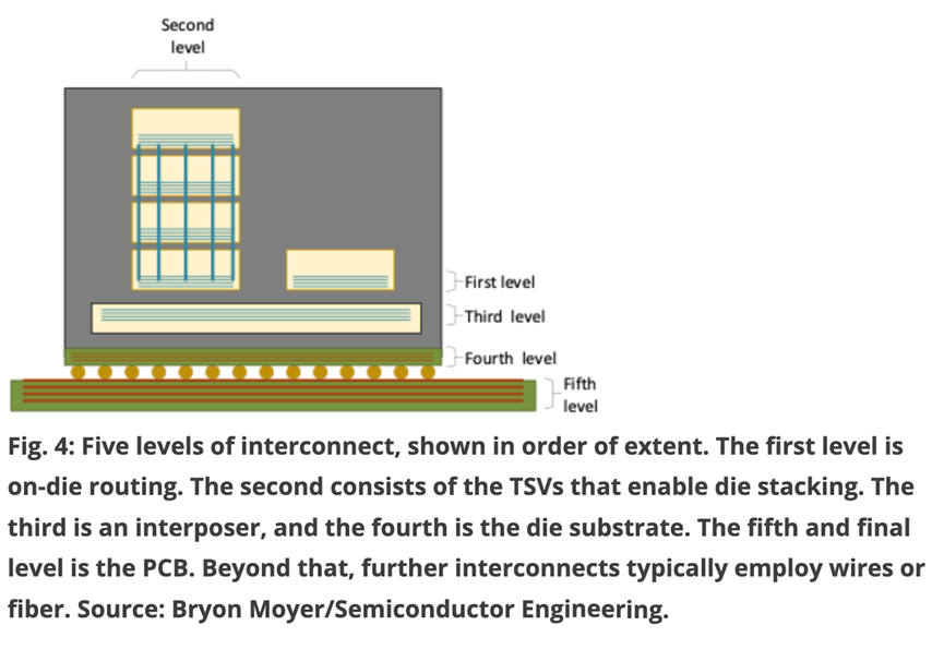
For decades, electronic devices have typically employed a two-level routing architecture to manage signals generated or terminated in integrated circuits. In recent years, the number of routing layers has increased to five. While this has significantly improved the structural flexibility of electronic devices, it has also introduced greater complexity and increased the number of decisions required to complete a project.
This shift has been gradual, not revolutionary. Developers have been finding solutions step by step, overcoming obstacles as they arise, and progressing incrementally. Like the story of the frog in slowly boiling water, we gradually adapt to each change until we can truly realize the profound impact of the cumulative changes only when we look back and compare the present with the past.
Starting point
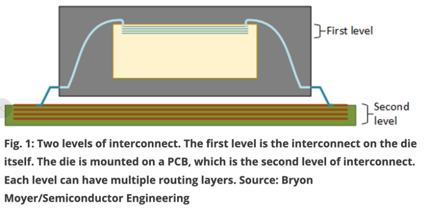
For the purposes of this article, the wiring "structure" or "platform" is defined as the location of the interconnect. Historically, these two platforms have been the metal wiring of the integrated circuit (IC) itself and the metal wiring on the printed circuit board (PCB). Both provide multi-layer wiring to maximize connectivity while mitigating the cost of adding wiring layers. The terms "layer" and "level" must be used with caution here because ICs and PCBs are two levels of interconnection, each of which can contain multiple wiring layers.

Until recently, the differences between the chip and PCB levels were significant enough to be discussed separately. Chip designers were responsible for building the internal wiring of the chip, while PCB designers were responsible for building the wiring that connects the integrated circuit to other board components.
At these levels, and all others, there are trade-offs between line spacing and the number of layers. Increasing the number of layers increases cost but can alleviate wiring pressure at certain levels. "While increasing the number of layers can reduce wiring density, it also increases patterning complexity and increases sensitivity to lateral etch effects," says Daniel Soden, product manager for lithography materials at Brewer Science. "Larger line spacing and more forgiving structural designs help balance these trade-offs."
Two options are too few
Three developments have challenged this simple approach:
The increased performance has made signal transmission lines more critical than ever before. Excessively long lines degrade performance, and traditional interconnect solutions offer two interconnect scales—chip-scale (line dimensions measured in nanometers) and PCB-scale (dimensions measured in micrometers and millimeters). These differences can be up to six orders of magnitude. In reality, there is no intermediate state between the two.
The second trend is the increase in chip power. When power reaches the kilowatt level, the generated heat becomes more difficult to dissipate. In older packages, the primary heat dissipation path was through the lead frame to the metal traces on the PCB. A more challenging scenario was adding a heatsink on top of the chip package. However, this approach has proven increasingly inadequate for heat dissipation requirements.
The third trend stems from the increasing chip integration, meaning that more circuitry can be integrated into each chip, whereas in earlier, simpler packages, more chips could be integrated onto each PCB. This exacerbates the power problem, causing power density (i.e., power per unit area or volume) to increase faster than power itself. High power density intensifies the heat dissipation challenge, as more heat must be dissipated from a smaller volume.
Enhancing the effectiveness of packaging
As chip size increases, the required number of I/Os also increases, and leadframes have proven insufficient for heat dissipation. In contrast, flip-chip packaging flips the chip over, using bumps instead of leadframes, and crucially, it connects the chip to the package substrate instead of the leadframe.
The substrate is essentially a miniature PCB made of organic materials, with dimensions far exceeding those of a standard PCB. The simplest substrates have only one layer, but multiple layers are also possible, making it a completely new interconnect solution.
The substrate is now an integral part of the packaging design. Traditionally, packaging design and chip design were separate, with critical information passed between them.
The traces on the substrate can be denser than those on the PCB. This has advantages and disadvantages. Shorter traces can improve signal quality, but narrower, denser traces do not. Thermal design is similar to the leadframe version, but the substrate provides more I/O interfaces, allowing heat to be transferred from the substrate to the PCB. Heat sinks (or more advanced cooling methods) can still be used if necessary.
Multiple chips can be mounted on the substrate, provided the area and line spacing allow.
Stacked package
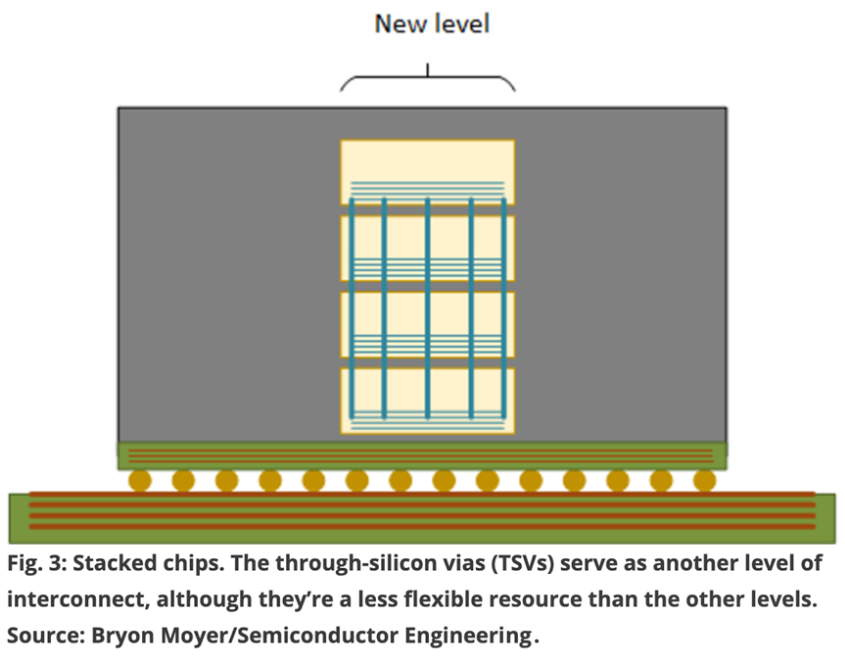
Another obvious way to improve packaging efficiency is to stack multiple chips in a 3D manner. The interconnect used to achieve this stacking is through-silicon vias (TSVs), which allow signals to travel vertically between chips. Compared to other interconnect methods, TSVs are less flexible because each TSV can only carry one signal.
While multiple TSVs exist, they are not routing resources available for specific routing algorithms. The location of TSVs can be flexibly adjusted, but the signals they carry are fixed. That is, choosing which signals reside on different TSVs is part of an overall partitioning process that breaks down a large problem into smaller ones. For some chips, such as HBMs, these signals may be obvious. But in most cases, this is not the case.

Chip stacking significantly increases the difficulty of heat dissipation because the chip located in the middle of the stack lacks a heat dissipation path. With a single chip within the package, heat can dissipate through any of the chip's six sides, especially the top and bottom. However, in such a stacked structure, the chips above and below each other generate their own heat - even if adjacent chips attempt to dissipate heat upwards or downwards, this heat is still transferred to the adjacent chips.
Effectively dissipating heat has always been a major challenge for such stacked structures. The materials surrounding the stacked structure may be modified to dissipate heat more from the sides, rather than relying solely on the top and bottom.
The height and strength of the stacked structure depend on the bonding technology. Currently, traditional microbump interconnect technology dominates, but hybrid bonding technology is making significant progress. "Hybrid bonding is a higher-performance solution - but also more expensive," notes Vikas Gupta, Director of Engineering and Technology Promotion at ASE Group.
The intermediary layer constitutes the fifth layer
Almost simultaneously with chip stacking technology developed 2.5D integration technology, which utilizes an interposer as an intermediate "PCB" with a much smaller line spacing than that on a PCB or substrate. Multiple chips or chipsets can be mounted on the interposer instead of the PCB. The main difference is that only packaged units are mounted on the PCB, while bare chips are mounted on the interposer or substrate. The line spacing on the interposer can be even smaller than that on the substrate.
Interposers can be organic materials like those on a PCB, or they can be silicon. The latter allows for finer dimensions, while the former is less expensive. They can have multiple wiring layers, currently around four, but this is expected to increase to eight or nine. Without an interposer, a single chip or stack would send all I/O signals from the package to the PCB. With an interposer, many signals no longer pass through it.
There are two ways to transmit signals solely through the interposer. The obvious advantage is that chips that might have been on the same PCB can now be located inside the package, and their connections are completely hidden.
A less obvious advantage is that what was originally a monolithic chip can be divided into multiple smaller chips. "You're taking apart a very large SoC and trying to break it down into smaller chips and chiplets," said Shawn Nikoukary, senior director of SoC engineering at Synopsys. "You're doing this to improve power consumption, performance, and area (PPA)."
Internal signals that might otherwise remain on a single chip can now be output from one chiplet to another. The line spacing on the interposer is narrower than the line spacing on the chip itself, but the silicon interposer can still provide narrow lines and narrow spacing - although their resistance may be high.

As the thickness of the interposer increases, mechanical warpage becomes a major challenge, caused by the different coefficients of thermal expansion of the multilayer materials. "The metal layer thickness is approximately 1.5 to 2.0 micrometers," explains Pax Wang, Director of Advanced Packaging at UMC. "The total thickness of the dielectric layers on the silicon substrate is approximately 15 to 20 micrometers. Traditional silicon processes significantly increase wafer warpage."
Cost is also a challenge; silicon interposers (with the smallest line spacing) are more expensive than organic interposers. If substrate design rules allow, abandoning the interposer and using the substrate directly might be helpful. "Replacing the interposer with the substrate would be a more cost-effective solution," Wang says. "The line spacing of the substrate is approximately 25 to 50 micrometers. In contrast, the line spacing of organic interposers is approximately 2 to 5 micrometers, which makes interposer architectures still highly practical for high-performance computing applications."
The island collapses
The design and verification process for five-layer interconnect systems is far more complex than it was decades ago, when chip and package designers worked independently. While PCB design remains separate, four of the five interconnect layers are located within the package, meaning the entire package must be designed and verified together.
Even seemingly trivial questions, such as whether the package needs a cover, must be evaluated, especially when planning thermal solutions. "Some customers want the package to have a cover," says Mike Kelly, VP of Chip/FCBGA Integration at Amkor. "This is very beneficial for improving mechanical strength, especially in testing and assembly line handling. But other customers have had to forgo the cover and place the thermal solution directly on the back of the chip."
These interconnect layers offer the greatest flexibility in the early stages of architecture design. If the design process involves splitting an original monolithic design, the simplest approach might be to start at the module level and determine where to split. However, the routing resources at each layer have a significant impact on routing performance. Some partitions will have better routing performance than others.
There is still more content that needs to be verified
Verification begins early and extends far beyond routing performance. "First, we do structural material analysis, such as RDL stacking requirements, material stacking, and their characteristics," said Cao Lihong, Senior Director at ASE Group. "Then, the goal is to perform pre-analysis, including layout planning, warpage analysis, and electrical simulation."
Satya Karimajji, Senior Engineer of SoC Engineering at Synopsys, agrees. "You can focus on the architecture level: What is the power consumption? What is the heat flux? What cooling methods can we expect to use? Assessing chip-level thermal integrity is also very helpful. We can improve thermal design by optimizing the materials used, module layout, stacking methods, etc."
But this isn't just about the chip itself; it also includes multi-layer mechanical packaging. "Another layer is the packaging itself, that is, the location of the package and the PCB, and airflow—or liquid cooling, or whatever thermal management methods we use," Nikoukary added.
Because these additional considerations go far beyond functional verification, the process requires multiphysics tools. These considerations, which used to be handled separately, are now part of the entire chip design flow.
Whether due to increased integration or monolithic decoupling, each chip will still have its own design team, just like before. However, their specifications cannot be determined until the higher-level architecture is finalized. Design teams can independently develop their individual chips or chipsets, but integrators must integrate these individual designs to ensure they work together.
The integration team's tasks include not only verifying functionality but also verifying robustness to physical characteristics such as signal integrity, power integrity, warp resistance, and overall thermal performance. These verifications have already been completed through estimation. Now, final verification is needed to confirm the design results.
Power surge
The increase in interconnect layers also enables more refined power delivery and signal quality solutions. Previously, voltage regulation was limited to the system level, delivering power to the board via wires; now, voltage regulation is being moved as close to the chip as possible, including placing voltage regulators inside the package. They can be mounted on the substrate or interposer.
Using decoupling capacitors (decapacitors) to buffer voltage fluctuations also improves signal integrity. In earlier single-chip designs, these decapacitors were typically located on the PCB near the regulator and chip (potentially small on-chip metal-oxide-semiconductor (MOM) or metal-insulator-metal (MIM) capacitors). In advanced packages, these decapacitors can be moved below the package, on the substrate, or on the interposer. New technologies also allow them to be integrated into the core layer of the substrate or interposer.
In other words, these interconnect layers—chip, stack-up layers, interposers, substrate, PCB—all provide opportunities to bring power and decapacitor circuitry closer to the chip. Currently, this design is not typically used at all five layers, but this possibility remains for future performance optimization.
The results of years of development
Rather than a revolutionary change, this is more of an opportunity to look back and examine the results of years of incremental improvements. Each improvement brought its own challenges. However, taken together, we handle simple, traditional chips very differently from new, complex chips.
This five-layer architecture may or may not influence our daily decisions in developing new chips. But at the very least, it gives us a clearer understanding of the extent to which chip flexibility and complexity are increasing. This way of thinking is especially important at the architectural level, where all layers can potentially play a role.
Source: Compiled from semiengineering


