
When it comes to device interconnects, it’s actually hard to beat copper wire. Because of its low resistivity and high reliability, it provides the industry with excellent on-chip interconnect and chip-to-chip routing. But in logic chips, as interconnect stacks move up into the 14-level range and resistance-capacitance (RC) delays become an increasing percentage of total delays, fabs are looking to alternative metals to maintain performance.
One option to reduce RC delay and help shrink standard size cells is backside powering. This somewhat radical proposal powers devices through the back of the chip rather than the front, relieving interconnect congestion and improving power transfer. The second option is hybrid bonding, which offers several advantages, including the ability to combine different devices with minimal latency.
Before IBM developed the dual damascene method for depositing copper interconnects into lines and vias, the industry used aluminum in a subtractive deposition and etch scheme. Today, copper interconnects have reached their scaling limits due to the impact of the liner metal (usually cobalt) and the barrier layer on resistivity. Alternative metals do not require liners or barrier layers, but their integration may require a transition back to deposition and etch processes. This change in integration scheme represents a huge change in the interconnect process—dual damascene on wide interconnects and subtractive etch schemes on narrow interconnects will run on the same production line. Ruthenium and molybdenum appear to be the best candidates to replace copper, and are expected to be implemented first in buried word lines in DRAMs or in the finest metal layers of logic devices.
“Controlling the oxidation of the metal during and after etching will be a great challenge, especially when using high-aspect-ratio metal lines for lower resistance, integrating air gaps between lines is desirable,” TEL Senior Technician and Technical Director Robert Clark said. air is the ultimate low-k material (k = 1.0), but it sacrifices structural support, unlike low-k dielectrics (3.3) and silicon dioxide (3.9). Nonetheless, leading chipmakers and tool suppliers are pursuing subtractive Ru and Mo etching with air gaps as the dielectric. Of the two metals, ruthenium is less prone to oxidation and is therefore better suited for etching and cleaning processes. Molybdenum, which oxidizes easily, is more compatible with mosaic flow.
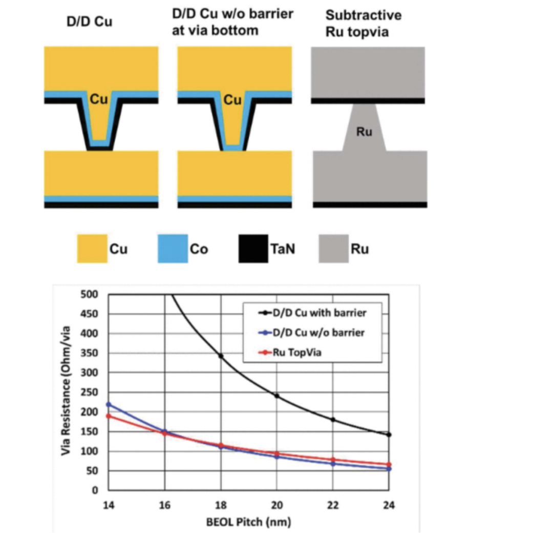
IBM and Samsung have developed a ruthenium and air gap integration solution that solves a looming problem of high interconnect spacing. “One of the challenges we had was that when we tried to CVD fill these narrow pitch lines, we ran into line wiggle,” said Chris Penny, a senior engineer at IBM Research. “We start looking at the cohesion that pulls the lines together, and you get dramatic CD changes or line collapses, and we showed that at IITC.” Penny described a via-top process flow using a spacer pull approach, which is similar to double patterning in dual damascene. A self-aligned litho-etch-litho-etch (SALELE: self-aligned litho-etch-litho-etch) step forms the top vias and bottom metal lines. “We transferred the pattern directly onto the ruthenium, so it has a lot of flexibility in the design space,” Penny noted. “You’re not limited to narrow lines, you’re not limited to wide lines.” To scale the copper process as much as possible, chipmakers are removing the barrier metal deposition (TaN) at the bottom of the via, which has a significant impact on via resistivity. The IBM/Samsung team demonstrated 18nm-pitch ruthenium wires and surrounding air gaps with aspect ratios as high as 4:1.
Another disruptive change involves backside powering (BPD)—moving power to the backside of the wafer so that the interconnect layers above the transistors carry only signals. The reason for the split is because power delivery and signal transmission have different needs. The power supply ultimately follows the low resistance path (thicker wire), but the high current makes it susceptible to electromigration. For signals, engineers want low capacitance and small cross-section, but some resistors are fine. With 12 to 14 metal levels in advanced logic, the power density goes up and the supply voltage (IR drop) is significant.Imec’s BPD approach uses fine-pitch nanoTSVs (200nm pitch, 320nm deep) extending down from metal-0 and landing on buried power rails with tight overlay control. They achieved this using finFET test equipment by bonding the front side to a carrier wafer, thinning the wafer, and then etching and filling TSVs. The IR drop is further reduced by incorporating a backside decoupling capacitor (metal-insulator-metal capacitor). The design is scalable beyond the 2nm node because TSVs do not occupy standard cell area.
BPD can reduce the number of tracks in standard cells. In addition to imec’s approach, there are two other backside power transfer schemes with increasing process complexity. All three face the challenge of thinning wafers down to ̴10µm. They need to align the backside with the frontside connections, and worry about series resistance — especially if the chips are stacked. But once the backside power distribution network is established, chipmakers now have another degree of freedom to integrate passive or active components on the backside.
Perhaps the most dramatic change in interconnect density has to do with hybrid bonding. In fact, hybrid bonding is being used to achieve rear side power distribution. Hybrid bonding involves the bonding of copper connections and the surrounding dielectric, with 1,000 times more connections per unit area than copper microbumps. Wafer-to-wafer (W2W: Wafer-to-wafer) hybrid bonding is more mature than die-to-wafer (D2W: die-to-wafer) hybrid bonding. “Chip-to-wafer alignment is much more complicated because you are managing the position of the four corners of the chip rather than the overall position of the two wafers,” said Thomas Uhrmann, chief technology officer at EV Group. Wafer-to-wafer bonding The underlying die most commonly used to bond pixel arrays into camera image sensors. “Hybrid bonding changed the game for image sensors in 2010. YMTC was the first NAND supplier to do hybrid bonding. In fact, most NAND flash memory companies that do hybrid bonding today have first in image sensors.” experience in hybrid bonding,” he added.
The key process steps of hybrid bonding include electroplating (ECD: electroplating), CMP, plasma activation (plasma activation), alignment, bonding, singulation and annealing. Although these tools are well established, for example, for the fabrication of dual damascene copper interconnects and flip-chip bonding, these processes need to be refined to meet the needs of hybrid bonding. These include <100nm alignment accuracy, new levels of cleanliness for die-to-wafer bonding and debonding tools, excellent CMP planarity with 0.5nm RMS roughness, and electroplating for optimal bonding.
While fabs are bonding nearly completed devices to each other, chipmakers are already looking to use hybrid bonding at the transistor level, allowing, for example, GaN to be combined on silicon.
“When you start to get to the point where hybrid bonding is used to combine transistors, it gets really interesting because now you’re at a much tighter pitch than what we’re looking at,” said industry analyst Dean Freeman. “Intel and other companies have done work combining GaN with silicon, which is very interesting. This is a great opportunity for RF in communications equipment because now, you have logic combined with the speed of GaN — Or eventually silicon carbide, or maybe even another material—works its communications side into the terahertz wavelength range, and then starts blowing millimeter waves out of the water we’re getting with our current 5G technology.”
The major shift from SoCs to multi-chip packages and systems has literally shifted performance, power, and cost metrics from the chip to the system. “Performance issues are no longer just silicon issues,” Freeman said. “The question about how we stack these little chips and how we manage to dissipate heat has now entered the packaging stage? Power management always seems to be our Achilles’ heel.”
Heterogeneous integration refers to the integration of different device technologies, such as co-packaging of optics and logic, 2.5D microprocessor and HBM, and 3D-IC that can bind memory, logic, high bandgap devices, RF, etc. are typical example. “This is critical to bringing emerging applications into the mainstream through enhanced performance, lower power requirements and improved cost-efficiency,” said Steven Hsu, vice president of technology development at UMC.
Mike Kelly, vice president of advanced packaging and technology integration at Amkor, said 2.5D and 3D integration will extend to all semiconductor applications. “However, the challenges will differ between low-cost applications and the high-performance market. Low-cost applications will require innovation to enable high-volume production.” “The transition to chiplets means high-bandwidth interfaces between these chiplets, This is the driving force for advanced packaging. High bandwidth and small die size require high signaling speeds and often wide interface buses,” Kelly said. “The latter puts considerable stress on smaller chip bumps with tighter bump pitches. This in turn requires more advanced equipment to achieve good alignment between die and interconnect. High-precision placement, At the same time maintaining high throughput is very important.” He added that high speed requires the industry to continue to push the development of low-k dielectric materials.
When companies are generally not open to sharing data about their chips, the question of how to assemble chiplets in multi-chip packages that contain chiplets from different manufacturers may be resolved through consortiums that have sprung up across the industry. “It’s going to be a few big companies, and then they’re going to push some type of platform or footprint, and they’re going to do it together,” said Chip Greely, vice president of engineering at Promex Industries. “Then everyone else is going to be looking on the outside and saying, ‘How do I get in?’ I envision three or four of these consortiums. And then the most powerful company will take over at the end. But in the meantime, you have the chiplet idea, which can still be very practical. With flip-chip, We can easily put many chips into the same substrate and put them together with the metal RDL to connect all the interfaces, because the fundamentals of assembly—die attach, flip chip, and wire bonding—haven’t changed.”
The lines between front-end and back-end processes are not as clear as they used to be. “The traditional boundaries between FEOL and BEOL are blurring as 3D packaging, W2W/C2W bonding, and the continued shrinking packaging density of chip-to-die interconnects continue to gain traction,” said UMC’s Hsu. “This means that FEOL and BEOL will be competing head-to-head in these highly competitive areas, and in fact we have seen foundries gradually expand their services to include traditional OSAT functions, especially in advanced product areas. Longer term , the high integration of FEOL and BEOL will be a necessary condition to realize a high-performance system, which will have an impact on the future industry pattern.”
Dev Gupta, APSTL’s chief technology officer and chair of the packaging integration segment of the International Roadmap for Semiconductors and Devices (IRDS), cautions that any technology forecasts of packaging trends should reflect knowledge gained in the past. “About two-thirds of all technologies used in advanced packaging today were invented by Motorola and Intel decades ago.” these patents. “In 1995, thermocompression bonding was used for robotic assembly of GaAs RF modules in mobile phones, and in 1998, laminated organic substrates entered high-volume production. Coreless organic substrates entered production in 2002 for use in servers.”
Gupta emphasized that the goal of advanced packaging for high-performance computing has been to minimize package losses, mainly from parasitic capacitance, as well as resistance and inductance. “New directions should be sought to minimize the impact on thermomechanical stress and reliability,” he said.
At the recent IEDM conference, Lihong Cao, Senior Director of Engineering and Technical Marketing at ASE, looked at the different market segments for Fan-Out Stacked Package (FOPoP), FO Chip-on-Substrate, and FOCoS Bridge. For high-density inter-die connections, bridge dies enable 0.8µm L/S to communicate between dies, especially in mobile packaging, high-performance computing, and AI/ML. On the other hand, she highlighted the continued usefulness of FOPoP as a key platform for compact, high-density integration—for applications processors, mobile antenna-in-package, and co-packaged silicon photonics applications. The absence of a substrate eliminates parasitic inductance and enables a thinner overall profile.
The biggest manufacturing challenges in fan-out packaging include die shift after mold (mold) and warpage. Warpage is caused by a mismatch in thermal expansion coefficients between materials. Amkor has qualified FO methods for up to 6 RDLs. Kelly didn’t predict the need for more than 6 layers, but he did expect RDL lines and spaces to range from 2µm today to 0.5 to 0.8µm. “While the lithography techniques required for submicron have existed for decades, newer versions of lithography equipment designed for packaging applications that can handle high warpage may be required,” he said.
In the next few years, silicon interposers may be replaced by organic interposers. “Despite their foothold in advanced packaging, Si interposers with Cu TSVs will gradually be replaced by organic interposers for reasons related to cost (i.e., availability) and high-speed performance characteristics. Over time, the The smallest usable feature size will be driven to sub-1µm line and space,” Kelly said.
Kelly also sees a need for 200mm wafer backgrinding and SiC wafer dicing equipment as the industry increasingly adopts larger wafers. “Most wafer bumping capacity in the industry is on 200mm and 300mm wafers. Before the recent introduction of SiC on 200mm wafers, it was very difficult to get 150mm wafers with flip chip bumping ,”He said.
Finally, the industry continues to gradually improve the thermal conductivity of thermal interface materials (TIMs) used between chip packages and heat spreaders, but these materials have a limit to their thermal conductivity. About 90% of the heat in a semiconductor package escapes from the top. TIMs are polymer-based materials with solid filter particles (alumina or silver) that increase conductivity depending on particle loading. However, Amkor’s Kelly points out that the thermal resistance of these materials is typically limited to 10W/mK in FCBGAs. The industry is evaluating graphite-based TIMs, he added. “Metal TIMs and solder, while used in packaging for many years, are penetrating broader market segments where thermal management has historically been less of a concern.”
As the industry increasingly adopts new interconnect materials, backside powering, hybrid bonding and advanced packaging, more will be learned about the manufacturing details of these processes. Minor improvements to copper interconnects, such as removal of the TaN barrier at the bottom of vias in copper damascene, will be made before all avenues are exhausted, especially if new integration schemes pose significant challenges.
Post time: Mar-28-2023