
Most discussions of advanced lithography focus on three elements—the exposure system, the photomask, and the photoresist—but that’s only part of the challenge.
The physical structure that successfully transfers the pattern from the photomask to the wafer also depends on the co-working of multiple thin films, including substrates, developers, and various surface treatments. In fact, most of the flexibility and adaptability of the process comes from these auxiliary materials, Samsung Electronics principal engineer Hyungju Ryu said in a talk at the recent SPIE Advanced Lithography and Graphics conference.
Lithography is the most complex development process, with exposure system development and procurement taking years. Therefore, changes to the photomask are undesirable once the design is in production within the fab. Therefore, optimizing pattern transfer for practical conditions usually falls on the photoresist and etch process.
The bottom layer normalizes the wafer surface
In any layer after the first layer, the device wafer exhibits an uneven surface. Oxide patterns interwoven with silicon and metal cause changes in surface energy and wettability, and previous surface treatments contribute to roughness.
Undercoating helps to smooth out this feature roughness and improve exposure results. They do this by normalizing the surface energy, promoting photoresist adhesion and reducing the risk of pattern collapse.
When thin photoresists are required, such as in high numerical aperture EUV, the photoresist layer itself may not capture enough exposure dose. A dense underlayer can help resist photoacid generator (PAG) diffusion, ensuring that the photoacid generator molecules remain close to the photoresist protecting groups. Unfortunately, EUV photons are so energetic that their reaction with the thin photoresist can excite secondary electrons from the underlying layer as well as from the photoresist itself. In metal oxide photoresists, the Applied researchers showed that these secondary electrons improve crosslinking, ensuring that the entire photoresist layer is insoluble in the developer.
Imec researcher Mihir Gupta points out that bottom layer design involves striking a balance between etch selectivity and corrosion resistance. Etch selectivity is the difference in etch rate between two materials. It depends in part on the interaction between the material and the etching plasma. The more different these materials are, the easier it is to determine the process conditions that will etch one but not the other.
A dense underlayer can improve selectivity by providing strong contrast with photoresist. At the same time, the total etching time is also an important factor affecting the erosion of photoresist. Dense underlayers etch more slowly, increasing the exposure of the photoresist to etching chemicals. Balancing these two factors becomes more challenging as resist thickness decreases.
Fabs typically use photoresists to pattern etch-resistant hard masks and then rely on the hard masks to protect the wafers. However, if the photoresist is too thin, it may be eroded away before the first transfer step is complete. As the photoresist thickness decreases, the bottom layer thickness should also decrease.
Unfortunately, as Brewer Science Senior Fellow Si Li and colleagues have shown, conventional spin-coating may not yield a uniform coating as the thickness decreases. Instead, Brewer Science engineers have demonstrated a small-molecule “spin-on-primer” material that can achieve thinner layers than conventional polymers.
Nissan Chemical researcher Wataru Shibayama and colleagues achieved similar results by first spin-coating the primer layer and then rinsing it with a solvent. The team then compared the results to purge cycles in atomic layer deposition. A solvent rinse removes unreacted primer, leaving a uniform thin layer (10Å).
Not all defects are printed: topcoat and developer As mentioned earlier, images captured by photoresist contain some degree of random defects. This is caused by photon and chemical shot noise, but this is not the end of the story, as not all defects captured by the photoresist are printed on the wafer. Even after exposure, there are many opportunities to improve the final printed pattern. For example, DuPont Electronics Technology Manager Hou Xisen and colleagues point out that ArF and KrF lithography processes often use topcoats after exposure and before post-exposure bake to chemically “trimming” the lithography by making defects and sidewalls more soluble in the developer. glue pattern.
The strength of the trimming effect is adjustable. It can simply reduce the probability of bridging defects, or the overall critical dimension (CD) can be adjusted. In EUV exposure tests, the DuPont team was able to reduce the required dose by 24% and still achieve the same resolution.
Dry resist and dry developer processes allow adjustment of resist and development parameters as part of the process recipe. Hyo Seon Suh, head of imec’s R&D team, explained that a more aggressive development process smoothed the line edges and eliminated some bridging defects. At the same time, a more aggressive process may make line breaks more likely. Typically, the post-etch failure-free window is centered on a larger CD than the photolithographic post-window.
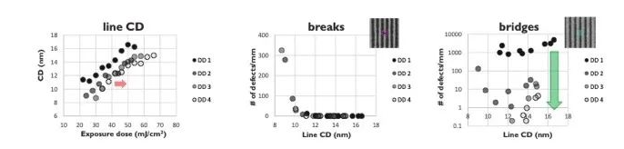
(Development) Optimizing dry development parameters improves roughness and bridging defects while modestly increasing the dose-to-size ratio.
In contrast, Inpria’s metal oxide resists rely on a wet rail-based development process. In their resist, protective ligands surround the metal oxide core. By co-optimizing resist and development chemistries, fabs can tailor the resolution/linewidth/dosage tradeoff to their requirements.
According to TEL researcher Cong Que Dinh, the key parameter to consider is m, the concentration of the dissolution inhibitor in the resist. The variation of m with depth ( dm/dx ) is a measure of complete or incomplete exposure. The standard deviation σm is a measure of resist segregation and other contributing factors of chemical shot noise.
In general, reducing the exposure dose increases dm/dx. The surface of the resist may be completely soluble, but incomplete development results in scumming at the bottom of the vias and scumming at the bottom of the resist features. Decreasing σm helps to improve contrast and sharpen feature edges. In TEL’s ESPERT process, developer chemicals reduce σm by changing the polarity of the exposed resist surface to facilitate dissolution. The TEL group was able to resolve 8nm half-pitch features printed by interference lithography. At 10nm half-pitch, sensitivity was improved by 30% and linewidth roughness was reduced by 21% through optimized development chemistry.
As the process evolves, imec’s Hyo Seon Suh says the absolute resolution achievable by exposure tools is the first step, followed by an etch system that can achieve that resolution on the wafer. But to truly realize these capabilities in production design, the ground floor, developers, and other lesser-known elements of the process play a key role.
Post time: Apr-26-2023