
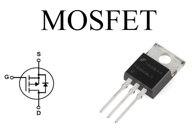
Over the past few years, the chip boom has drawn attention to the semiconductor industry. Among them, transistors and MOSFETs are the basic components of chips, and we have read many reports from many articles. In this article, we explore the origin and past life of MOSFETs in detail.
Early exploration of FETs
The first wave of semiconductor companies began in April 1952 when Bell Labs held its second transistor symposium for licensing its transistor patents, with representatives from about 40 companies. After the workshop, most of these companies started manufacturing bipolar contact transistors within a few months or a few years, and many became successful commercial semiconductor suppliers. Among them were Infineon (formerly Siemens), NXP (formerly Philips) and Texas Instruments – which still make semiconductors today. In contrast, the development of metal-oxide-semiconductor (MOS) field-effect transistors (FETs) took decades, from an idea in the 1920s to initial working devices in the late 1950s to commercial products in the 1960s . It took years of scientific research, engineering design, analysis, and a fair amount of publicity to transform this largely neglected device into the backbone of today’s semiconductor and electronics industries.
Julius Edgar Lilienfeld was the first to patent the idea of the FET. Lilienfeld was born in 1882 in the city of Lviv, now located in the western part of Ukraine. At that time, it was part of the Austro-Hungarian Empire. On February 18, 1905, he received his doctorate at the Friedrich-Williams University (now Humboldt University) in Berlin, and then became a non-tenure professor at the Institute of Physics there. His research focused on electric fields and the emission of electrons induced by fields, and his early work centered on the wonder device of the time: the X-ray tube. He also did some early work on the behavior of electrons in high electric fields that was eventually thoroughly analyzed by physicists Ralph H. Fowler and Lothar Wolfgang Nordheim.
Lilienfeld first traveled to the United States in 1921 to defend his X-ray patent against its seizure by alien custodians in 1919. He emigrated permanently to the United States in 1926 to escape growing anti-Semitism in Europe. In October 1926, he filed the first of three patent applications based on his experiments in the field of semiconductors. These patents basically described the conceptual basis for FET operation and were issued between 1928 and 1933. Lilienfeld held a research and development position at Amrad (Radio and Research Corporation of America), a radio parts manufacturer in Malton Hills, Massachusetts. There he studied the electrochemistry and behavior of anodized aluminum oxide films, and his detailed analysis of these films formed the basis for the manufacture of electrolytic capacitors for decades. Although three of Lilienfeld’s patents described the conceptual operation of field-effect transistors, the state of the art in semiconductor processing at the time produced materials of far less purity than would be required to manufacture such devices.
Oskar Heil was the second person to conceive of the FET independently. He was born in Longwitten, Germany in 1908 and received his doctorate at the Georg-August University in Göttingen. While at the university, he met Agnesa Arsenjewa, a Russian physicist who was working on a Ph.D. The two married in the Soviet Union in 1934 and moved to the British Cavendish Laboratory in Cambridge. Together, they co-authored a seminal paper on generating microwaves. They continued this work at the Institute of Physical Chemistry in Leningrad. Heil then returned to England without Arsenjewa. While working at the University of Cambridge in 1934, Heil applied for a patent on the control of electric current in semiconductors by capacitive coupling on electrodes, an essential element that defined FETs. The patent was entitled “Improvements in or relating to electrical amplifiers and other control arrangements and devices” and was granted in late 1935. However, the low purity of the semiconductors available at the time and the complete absence of the necessary fabrication process technology would again hinder the practical realization of such a device, and there is no indication that Heil ever attempted to make a field-effect transistor.
When the German invasion triggered World War II, Heil returned to Germany and began developing microwave generators for the C. Lorenz company in Berlin-Tempelhof. There is a persistent myth that Heil not only succeeded in making FETs, but used FETs to build a secret radio during World War II, but there is no evidence that Heil ever tried to make FETs. To make this myth a reality, Heil would have to figure out how to make a working field-effect transistor, and then needed to design a circuit for a field-effect transistor-based radio in the era of tube radios. If you wanted to build a secret AM radio in the 1940s, it was much simpler to make an audio detector using a variable inductor, a capacitor, a lump of galena, and a steel cat’s whisker, and the same efficient. In addition, Heil works in a microwave laboratory in Germany. He had access to as many vacuum tubes as he wanted. It’s highly unlikely that he wanted to build FETs so he could build a radio.
Although Lilienfeld and Heil both conceived of the FET, it’s no more accurate to say they invented the FET than to say Leonardo DaVinci invented powered flight. According to the Smithsonian Institution’s National Air and Space Museum, DaVinci created more than 35,000 texts and 500 sketches about the aircraft. However, we credit the Wright Brothers with inventing the first powered airplane because they built and flew the first of its kind.
The advent of the transistor
William Shockley was born in London, England in 1910. His parents were American. He went to school at the Massachusetts Institute of Technology. He received his Ph.D. in 1936, specializing in solid-state physics. In the same year, Bell Laboratories hired him to conduct research to explore the possibility of using crystalline semiconductors to manufacture solid-state amplifiers. In 1939 Shockley wrote: “Today it occurs to me that an amplifier using semiconductors instead of a vacuum is possible in principle.” Shockley seems unaware of the earlier patent granted to Lilienfeld and Heil.
Shockley and Walter Brattain unsuccessfully developed a FET before World War II began. The war put a temporary halt to this work, but after the war Shockley added John Bardeen to the team. Through a series of physical experiments, Brattain and Bardeen finally created a working point-contact transistor on December 16, 1947, with a gain of about 100 across the audio frequency band. However, as it happens, this first transistor is not a FET. It is a bipolar transistor and does not operate based on an electric field.
Bell Laboratories announced the invention of the transistor on June 30, 1948. The six-month delay gave Bell Labs’ patent attorneys time to get the patent application done. Before Brattain and Bardeen’s breakthrough, Shockley had moved away from his day job and was more of a consultant and manager, but now that the feat has been accomplished, he’s ready to be part of the team again and insist on being part of any PR photo shoot. He always stands front and center. He also decided to work on his own patent application, insisting that the transistor he had created was a FET. Bell Labs patent attorneys refused to work on Shockley’s patent application because it was too similar to Lilienfeld’s patents of the late 1920s and early 1930s, and they removed his name from Bell Labs’ patents for the same reason. Removed from the original transistor patent.
After the demonstration of the transistor in June 1948, Shockley spent a frantic month theoretically analyzing its workings. He determined that the transistor action of the point contact device comes from the P-N semiconductor junction. Based on this insight, Shockley quickly conceived the sandwich transistor, the first of a new breed of device known as the junction transistor. If you see a simplified diagram of a bipolar transistor, it usually depicts a sandwich transistor with the base as the sandwich fill between the transistor’s emitter and collector.
When Bell Labs announced the junction transistor in 1951, it quickly became the industry’s dominant transistor because it was superior in every way to the original point-contact device. However, it’s still a bipolar transistor, not a MOSFET. In 1950, Shockley poured his analysis into the first major book on semiconductor transistors, Electrons and Holes in Semiconductors: With Applications to Transistor Electronics. This book has been the bible of the semiconductor industry for many years. Shockley, Bardeen and Brattain shared the 1956 Nobel Prize in Physics for their research on semiconductors and their discovery of the transistor effect.
Frustrated by the lack of promotion at Bell Labs, Shockley moved to his hometown of Palo Alto, California, and in 1955 formed his own company, Shockley Transistor Laboratories. He was not working on MOSFET development there. He had moved on to bipolars and became fascinated by a Bell Labs project, the 4-layer diode. Shockley Transistor Lab licensed Bell Labs’ transistor patents, and Shockley himself continued to maintain close ties with Bell Labs researchers, bringing many semiconductor process innovations to the San Francisco Bay Area that would quickly lead to the establishment of Silicon Valley.
Mohamed Atalla and Dawon Kahng of Bell Labs became the first to build a working MOSFET. Atalla was born in Port Said, Egypt. He studied at Cairo University, Egypt, and received his MS and Ph.D. degrees from Purdue University, USA. Atalla joined Bell Labs in 1949. Dawon Kahng was born in Seoul, South Korea in 1931, before Korea was called South Korea. He studied physics at Seoul National University in Korea, immigrated to the United States in 1955, and received his doctorate at Ohio State University in 1959. In the same year he joined Bell Laboratories.
Atalla and Kahng’s development of the first working MOSFET was based on early research at Bell Laboratories by Carl Frosch and Lincoln (Link) Derick, who in 1955 accidentally discovered a method for growing a layer of silicon dioxide on top of silicon Methods. By 1957, Frosch and Derick had refined the idea and added the concept of using a silicon dioxide layer as a diffusion mask for silicon doping, which they published in the September 1957 issue of the Journal of the Electrochemical Society An article entitled “Surface Protection and Selective Masking During Diffusion in Silicon ” discusses this issue.
Importantly, the Bell Labs practice was to remove the silica layer after diffusion, as it was considered “dirty”, as in “carrying contaminants”. Two months after Frosch and Derick’s paper, Jean Hoerni of Fairchild Semiconductor realized the importance of the silicon dioxide layer and, for several reasons, it should have been left in place. The pure silicon dioxide layer becomes an integral part of Hoerni’s planar fabrication process and will be a key factor in the fabrication of integrated circuits.
Atalla has refined this discovery further into the more formal technique of silicon dioxide passivation, which, combined with newly developed photolithography and etching techniques, allows for more precise incorporation of silicon at specific locations. Using this technique, Atalla and Kahng succeeded in making a working MOSFET in early 1960, three decades after Lilienfeld first conceived the device. Although the device works to some extent, there are several problems with this first MOSFET. Notably, it is 100 times slower than contemporary bipolar transistors, mainly because of its relatively large channel length of 20 microns.
Because this initial MOSFET was so slow, Bell Labs had no interest in it, and Atalla and Kahng got little credit for developing it. Despite the lack of credit and interest, Atalla and Kahng continued to study semiconductors and developed p-channel and n-channel MOSFETs, the first working Schottky diodes, and the first nanoscale layer-gate bipolar transistor, which Sandwiched between the gate and the emitter is a thin metal gate — only a few nanometers thick. The thin base structure allowed the transistor to operate at much higher frequencies than bipolar transistors of the time.
Tired of not being recognized for his work, Atalla left Bell Labs in 1962 to join Hewlett-Packard. He helped the company establish its own semiconductor laboratory – HP Associates, and became director of semiconductor research. He then helped found Hewlett-Packard Laboratories in 1966 and became the first person to direct its solid-state division. Atalla left Hewlett-Packard in 1969 to become vice president and general manager of the Microwave and Optoelectronics Division at Fairchild Semiconductor Corporation, where he spearheaded gallium arsenide material research.
Kahng remained at Bell Labs for many more years. He applied for a patent for the MOSFET in 1960 and received it in 1963. Together with colleague Simon Min Sze, Kahng developed the floating gate MOSFET in 1967. This invention is the core storage element used in EPROM and EEPROM. Kahng retired from Bell Labs in 1988 to become the founding chairman of the NEC Research Institute, now known as NEC America Laboratories, the U.S. center for NEC Corporation’s global network of corporate research laboratories.
Kahng remained at Bell Labs for many more years. He applied for a patent for the MOSFET in 1960 and received it in 1963. Together with colleague Simon Min Sze, Kahng developed the floating gate MOSFET in 1967. This invention is the core storage element used in EPROM and EEPROM. Kahng retired from Bell Labs in 1988 to become the founding chairman of the NEC Research Institute, now known as NEC America Laboratories, the U.S. center for NEC Corporation’s global network of corporate research laboratories.
Atalla and Kahng received the 1975 Stuart Ballantine Award from the Franklin Institute for their invention of the MOSFET. After decades of research that existed only in theory, they demonstrated that it is possible to make a MOSFET. However, the original equipment was problematic. They are slow, their characteristics change with temperature and time, and they are not reliable. No application needs a slow, unreliable transistor. The quest for better MOSFETs and suitable applications was embraced by MOSFET evangelists from several companies. Along the way, MOSFETs became faster and more reliable. When the dust settled a few years later, many people contributed to the ultimate success of the MOSFET, but it was not an easy journey. There are technical problems to overcome, corporate politics to navigate, and business hurdles to defeat.
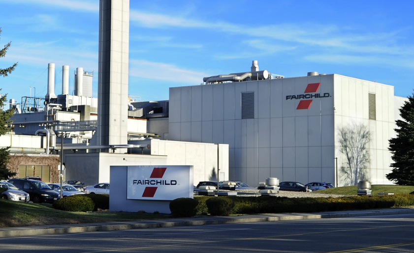
The ups and downs of Fairchild Semiconductor
No company is in a better position or position to take advantage of the development of the first MOSFET than Fairchild Semiconductor. The company was founded in 1957, engaged in the research of silicon transistors, Jean Hoerni developed the planar process, Robert Noyce proposed the first technology based on the Hoerni planar process a few months before Atalla and Kahng got the first MOSFET work at Bell Labs. A practical integrated circuit (IC) idea. Like the two keys needed to open the safe of a bank vault, planar semiconductor process technology and planar integrated circuits are the two keys needed to unlock the full potential of MOSFETs.
Fairchild Semiconductor held these keys, and despite the significant contributions of Fairchild researchers to the development and improvement of MOS, the company was unable to create a successful family of MOS integrated circuits. As a result, the company saw the disappearance of its early IC leadership, bipolar ICs, as Moore’s Law pushed IC device density beyond the range of bipolar transistor technology and into the alluring field of MOSFETs.
William Shockley left Bell Labs in 1953 because he felt neglected for promotion and recognition. He moved back to California, took a position at Caltech, struck a deal with Caltech professor and high-tech entrepreneur Arnold Beckman, and in 1955 founded the Shockley Transistor Laboratory. At first, Shockley thought he could raid Bell Labs personnel, but no one at his former employer was willing to cooperate with him. Forced to look elsewhere, he manages to assemble a superteam of young, freshly graduated scientists and engineers and lure them into California’s superweather. He also promised that they would develop today’s holy grail, the silicon transistor.

The following year, Shockley shared the Nobel Prize in Physics with John Bardeen and Walter Brattain for their invention of the point-contact transistor. Around that time, Shockley became interested in 4-layer diodes, semiconductor switches that would have been of great interest to Bell Systems. However, this wasn’t the device he had promised his researchers, and they weren’t happy. Shockley’s autocratic management style and ego split his team, leading to a showdown on May 29, 1957. The research group’s request was to solve the “Shockley problem”. It was not resolved, and eight members of Shockley’s research group – later known as the “Traitor Eight” – left in September 1957. This core group entered into an agreement with Sherman Fairchild Corporation to form Fairchild Semiconductor on October 1, 1957. Fairchild Semiconductor would quickly become the most important semiconductor company in the world, and the one most likely to bring the MOS transistor to its full potential.
The first major step toward realizing Fairchild’s fortunes was the invention of a planar semiconductor process. On December 1, 1957, just two months after Fairchild was founded, Hoerni had a sudden inspiration. He knew about the ongoing work at Bell Labs on silicon dioxide passivation, lithography, and etching because Shockley had discussed it with his research group earlier that year, before the “Rebel Eight” left this problem. Hoerni devoted just two pages in his lab notebook to describing the planar process. His innovation left thermally grown silicon dioxide on the semiconductor wafer after diffusion to protect the underlying circuitry. Bell Labs thought the oxide was too dirty to stay in place, but Houerney realized that a clean enough insulation would keep out dust, dirt, and water contamination. With few changes, Hoerni applied for a patent for the planar process on January 14, 1959.
The second major step towards the semiconductor breakthrough occurred on January 23, 1959, which was necessary to allow MOSFETs to fulfill their destiny. On that day, Fairchild Semiconductor founder Robert Noyce wrote down his idea for a monolithic integrated circuit in his lab notebook. He has been thinking about how to use Hoerni’s planar process to make more discrete transistors. He realized that the silicon dioxide layer was a perfect insulator, allowing metal interconnects to be deposited on top of it to connect multiple devices on an integrated circuit. With this flash of insight, Noyce changed the electronics industry forever and transformed soldering and wiring into a high-tech printing process.
These two ideas, Hoerni’s planar technology and Noyce’s integrated circuit concept, ignited Fairchild’s fuse. First, Fairchild uses a planar process to make better and more stable transistors than any competitor. Fairchild’s transistors quickly became the gold standard. Within two years, Fairchild Semiconductor announced the world’s first integrated circuit product family, known as Micrologic. This is a family of bipolar logic integrated circuits. In the six months since the introduction of the Micrologic family, Fairchild Semiconductor has swept the field. Fairchild’s competitors have nothing to offer their customers quite like Fairchild’s ICs. Even Texas Instruments, officially a co-inventor of the integrated circuit, had to license Fairchild’s integrated circuit patents in order to compete.
Soon after Mohamed Atalla and Dawon Kahng got their first device working in 1960, Gordon Moore learned that Bell Labs had successfully developed the first MOS transistor. In 1959, after Robert Noyce became the company’s general manager, Moore took over as director of Fairchild Semiconductor’s research and development department. Edward Baldwin, who was hired to hold the position at the time, suddenly left with five other Fairchild Semiconductor employees and founded Rheem Semiconductor.
A week after Baldwin left, Fairchild tested the first bipolar transistor made with Hoern’s planar process. This transistor works fine. One theory is that Hoern spat on the transistors during testing to demonstrate that the planar process kept the transistors free from contamination. Perhaps the actual tests performed were less ostentatious and did not use samples of Hoern’s saliva, but the planar process did have the desired effect. “Gee, Baldwin had to leave last week, it’s too bad,” recalls Jay Last, co-founder of Fairchild, which had been producing mesa transistors and within months moved production to a far larger Superior and more stable planar transistor design.
With the new planar bipolar transistors and Micrologic integrated circuits, Fairchild had a very fulfilling job making the planar process reliable and stable, learning to implement the precision lithography needed to make integrated circuits, and developing new bipolar transistors. polar transistors and Micrologic chips. No Fairchild customers asked or even asked for MOS transistors, so no one was developing them. Gordon Moore’s research and development department focuses on long-term projects, which do not include MOS transistors.
In 1962, Fairchild Semiconductor hired Frank Wanlass, a newly minted Ph.D. in physics from the University of Utah, to change the indifference to MOS. When he joined the company, Wanlass was already fascinated by MOS transistors, and he knew Fairchild’s planar process was the way to make MOS transistors.
Wanlass was hired into Fairchild’s R&D department, and his assignment gave him plenty of leeway to work on MOSFETs, even though Fairchild didn’t make MOS at the time, because whether it’s used to make bipolar or MOS transistors, MOS — metal Oxide-semiconductor-structures are all an integral part of planar processes. Much of his freedom comes from his ability to do almost everything by himself. As a physicist, Wanlass understood the physics of MOS structures so he could design MOSFETs himself. He knew electronics, so he designed not only transistors, but circuits that went into MOS integrated circuits. One of his earliest designs was an integrated MOS flip-flop with a flow rate of over 80%. In February 1963, Wanlass and his manager, C.T. Sah, published a paper at ISSCC revealing that Wanlass had conceived a circuit combining p-channel and n-channel MOSFETs on the same integrated circuit. He invented CMOS, which was just a by-product of his work.
In the process, Wanlass dealt with the inherent stability issues of MOSFETs and Fairchild’s general disregard for MOSFETs. The company was too good at making bipolar semiconductors that it put a lot of effort into slow MOSFETs. Although Gordon Moore’s R&D department put a lot of effort into analyzing and simulating MOS physics as a way to improve planar processes, those improvements were aimed at the fabrication of bipolar transistors. By December 1963, Wanlass was frustrated and jumped ship. He joined General Microelectronics (GME), which had been started in the summer of 1963 by members of Fairchild Semiconductor’s Micrologic group with the specific purpose of developing MOS integrated circuits.
With the loss of several key members of the Micrologic Group and Wanlass Corporation, Fairchild’s limelight was gone, and the company never developed a MOS IC product family. Eventually, Moore himself realized that Fairchild hadn’t realized the full potential of the MOSFET. When he left Fairchild with Robert Noyce to start Intel in 1968, it would have created a semiconductor company specializing in the production of MOS integrated circuits — specifically, memory integrated circuits — but that event has passed Nearly five years.
Birth of the MOSFET
In the early 1960s, it was not surprising that semiconductor companies were reluctant to invest heavily in the development of MOSFETs. Early MOSFETs were 100 times slower than bipolar transistors, and they were considered unstable for a reason: their electrical characteristics underwent severe, unpredictable drift over time and temperature. Turning MOSFETs into reliable electronic components required a lot of research and development.
However, the MOSFET found its supporters when Fairchild Semiconductor hired Frank Wanlass. Wanlass is committed to MOSFET research, not any company. He went everywhere and did everything to advance the development of MOSFETs. He became the Johnny Appleseed of MOS (Metal Oxide Semiconductor) technology, freely sowing the seeds of MOSFETs anytime, anywhere.
Fairchild hired Wanlass in August 1962, while he was earning a Ph.D. in physics from the University of Utah. He became interested in MOS technology when he read about RCA’s work on thin-film cadmium sulfide (CdS) field-effect transistors while doing his Ph.D. in solid-state physics. The simplicity of the FET device structure first intrigued him, then fascinated him. He realized that the simple structure of field-effect transistors meant that many field-effect transistors could fit on a single semiconductor chip, and he envisioned building complex integrated circuits (ICs) from these devices. But RCA’s thin-film CdS FETs are too unstable. Even when left on a shelf for hours, their electrical characteristics can drift dramatically. Wanlass believes that making the FETs with silicon instead of CdS will solve the parametric drift problem. As it turned out, he was wrong. Semiconductor field effect transistors suffered from drift for several years until the MOS fabrication process could be cleaned sufficiently to remove contaminants that caused field effect transistor parameter drift.
When Wanlass joined Gordon Moore’s research and development group at Fairchild, the company had a policy of letting newly hired PhDs work on any project they wanted to take on. Wanlass decided to focus on MOSFETs, even though Moore’s department wasn’t particularly interested in making such devices. However, Moore’s department was very interested in MOS processing because of the fundamental structure and properties of Jean Hoerni’s planar fabrication process, which Fairchild used to make bipolar transistors and integrated circuits. Any further understanding of planar processes and any improvements in process technology will further improve Fairchild Semiconductor’s ability to manufacture bipolar transistors and integrated circuits.
Wanlass is not interested in studying or analyzing the characteristics of the MOS process. He wanted to make discrete MOSFETs, make ICs out of MOSFETs, and use these devices to design system-level circuits to foster demand for these components. Over the next year, he did exactly that. In less than six months, Wanlass designed and fabricated individual p-channel and n-channel MOSFETs in silicon using a planar process. All p-channel devices exhibit severe parametric drift, while n-channel devices do not work at all. He tested the parametric drift of the p-channel device by placing it in a curve tracer and heating it with a cigarette lighter. He then designed and fabricated a flip-flop IC using MOSFETs and achieved an incredible wafer yield of over 80%. He developed application circuits for MOSFETs, including an ammeter that took advantage of the MOSFET’s extremely high input impedance.
Along the way, Wanlass and his manager, C.T. Sah, patented the idea of a CMOS circuit that combined p-channel and n-channel MOSFETs on a single silicon chip. CMOS is the underlying transistor technology for nearly all integrated circuits manufactured today. (Note: Sah is often listed as the sole inventor of CMOS, but his name appears on the patent because he is the manager of Wanlass, and it is customary to list the manager along with the inventor in the patent application.)
In early 1963, Gordon Moore began to hire more people to conduct a more thorough analysis of MOS process technology. However, he was not interested in studying MOSFETs. He just wanted to better understand planar metal-oxide-semiconductor processes so Fairchild could make better bipolar transistors and integrated circuits. The analytics team became Bruce Deal, Andrew Grove and Ed Snow. They were not placed on a formal team, but they quickly discovered each other and their complementary assignments through casual interactions in the office. . Deal is engaged in the research of oxidation and surface state. Snow analyzed the transient instability of MOS. Grove wrote programs to simulate the analysis.
By the end of 1963, Wanlass was convinced that Fairchild only wanted to study and analyze MOS devices, not manufacture them commercially, and he preferred manufacturing devices to researching them. Wanlass left Fairchild Semiconductor in December 1963, just one year and four months after he joined the company. He worked at General Microelectronics (GME), which was started by a small group of ex-Fairchild employees who decided to form a semiconductor company. GME was one of Fairchild Semiconductor’s first spin-off companies, collectively referred to as “Fairchild.” The goals and direction of GME would obviously take Wanlass where he wanted to go, and Wanlass was immediately responsible for creating and manufacturing MOS transistors and ICs.
Wanlass brings his superb MOS design skills to GME. He successfully made MOSFETs and small MOS integrated circuits at Fairchild, so he brought those capabilities, but he also brought another important thing. While working at Fairchild, Wanlass discovered that if he evaporated aluminum interconnects on semiconductor wafers using electron beam evaporation instead of thermal evaporation, he could greatly reduce the time and temperature drift of MOS characteristics. Fairchild has been building electron beam evaporators in its basement. It was one of the first semiconductor companies to have this type of evaporator.
In an interview, Wanlass said: “I was driving on the 101 freeway one day, and it hit me on a Sunday. It must be sodium, and I sent some aluminum wire for spectroscopic analysis. I got it from my Known from university work, some of my thesis work, sodium… I know for a fact that sodium, with a little help from temperature and voltage, diffuses directly through quartz. It has a very high diffusion quotient. I know this. It was an experiment done at the university.”
Suspecting that the thermal vaporization process somehow deposited contaminated aluminum on semiconductor wafers that caused device drift, Wanlass tried evaporating platinum onto the wafer instead of aluminum. Platinum was not chemically etched, so he had to manually scribe the gates on the platinum layer with a pointed tungsten probe. The resulting MOSFET has almost no drift. Then he tried gold and other metals, but platinum was superior. Then, for completeness, Wanlass used an electron beam evaporator to place the aluminum on the wafer. They also didn’t drift as much, and e-beam evaporation of aluminum quickly became part of the MOS process recipe. This all happened while Wanlass was still at Fairchild, and he brought this important knowledge to GME.
Eventually the industry will understand that sodium ion contamination causes drift and kills p-channel MOSFETs over time while making it impossible to build working n-channel MOSFETs. Aluminum is contaminated with sodium when it is drawn through a wire die to make aluminum wire that is used as a raw material for vapor deposition. The wire die is lubricated with sodium. Electron beam vaporization uses a shutter mechanism that shields the silicon wafer from the crucible in which the aluminum is melted until the aluminum reaches its vaporization temperature. Sodium has a much lower boiling point than aluminum, so it boils and dissipates before the shutter of the evaporation chamber opens and exposes the wafer to the aluminum vapor.
Wanlass metallized the wafers at GME using an electron beam evaporator, and by May 1964 he had produced a working, discrete MOS transistor. The company pushed the device to commercialization months before Fairchild was able to do it. Wanlass then built a monolithic MOS IC with a 20-bit shift register, not because a customer asked for it, but simply because he could do it. The 20-bit shift register is a very good MOS IC demonstration carrier. At the time, the shift register was the industry’s preferred form of small digital storage device because of its low pin count while allowing the device to fit in a TO-5 metal can transistor package with as many as 12 pins.
Although GME had a booth at WESCON (Western Electronics Show and Conference) in Los Angeles in 1964, the company also rented a hotel room just to demonstrate Wanlass’ shift register integrated circuit. GME’s MOS shift register IC demonstration impressed potential customers, firmly established GME’s leadership in MOS ICs, and positioned Wanlass as an industry authority on MOS IC development.
GME’s demonstration of a MOS shift register integrated circuit, the company’s growing reputation as a MOSFET supplier, and the sales skills and connections of one of GME’s founders, retired U.S. Marine Corps Colonel Art Lowell, attracted customers from the U.S. government. The company’s first MOS design contract was with NASA to design an integrated circuit with six or seven MOSFETs for the Interplanetary Monitoring Platform spacecraft. Special NASA Goddard Space Flight Center management. Spacecraft have severe power constraints, so low-power MOS ICs seemed tailor-made for the project. The super-secret National Security Agency (NSA) also became an early customer of GME. Wanlass recalls that the NSA had an ambitious plan to put wireless communications with decryption circuits inside soldiers’ helmets.
Device density put GME on the path to the early destiny of MOS integrated circuits: the calculator. GME signed an agreement with Victor Comptometer to build a MOS calculator chipset consisting of at least 20 ICs, each containing hundreds of circuit elements, including MOSFETs. This should have been a dream project for Wanlass, but he could see that GME would not be up to the challenge. Wanlass left GME in December 1964, when the calculator project was just beginning. As he expected, GME’s calculator project has been plagued by delays. The company started having money problems and was bought by Philco-Ford in 1966. It became the Microelectronics Division of Philco-Ford Corporation, and the General Microelectronics brand name ceased to exist. Philco-Ford eventually abandoned the Victor calculator project in 1968, and a few years later Ford decided to sell it and the company itself ceased to exist. “GME collapsed because they didn’t have enough money and they pushed too fast, too fast,” Wanlass said in an interview.
When he left GME, Wanlass and four of his colleagues first tried to start their own semiconductor company, but the deal fell through. Instead, the team joined General Instrument (GI: General Instrument), an East Coast electronics conglomerate looking to add semiconductor manufacturing, specifically integrated circuit manufacturing, to its portfolio. GI has hired managers from other semiconductor manufacturers, including Philco and IBM. Join Wanlass and his team to define the direction of a new semiconductor division: MOS.
One of the first things Wanlass did at GI was design and manufacture a 21-bit shift register IC, one bit larger than GME’s device, so that GI could claim the largest device available. Soon, GI introduced 50-bit and 90-bit MOS shift register ICs. Then again, what Wanlass did during his tenure at GME gave him a return on investment. When Wanlass was demonstrating GME’s 20-bit shift register in a hotel suite at WESCON in 1964, he met an engineer named Bob Booher, who was working for Rockwell Automotive, an avionics contractor known especially for Known for developing inertial guidance systems for US submarines and ICBMs. During that meeting, Wanlass seemed to infect Booher with his enthusiasm for MOS integrated circuits.
A few years later, Booher approached Wanlass at GI and asked if GI could manufacture one of his designs. It was a Digital Differential Analyzer (DDA: Digital Differential Analyzer), a very ambitious device for its time. Booher’s DDA was a digital implementation of Vannevar Bush’s Differential Analyzer, a mechanical analog computer that was widely used to numerically solve differential equations before the advent of digital electronic computers. Eventually, Rockwell Controls would set up its own semiconductor manufacturing group, but that was in the future, and Rockwell couldn’t make chips that large at the time. The chip design required thousands of transistors and was the most complex integrated circuit design Wanlass had ever seen. Additionally, Booher has developed a novel 4-phase clocking scheme that results in fast dynamic logic gates while saving silicon space. Wanlass agreed to make the chip for Booher, and the device has been successful. In August 1966, GI presented the device, and Buch was ecstatic.
By 1967, Wanlass’s notorious impatience was once again on display. He made a deal he didn’t like, but this time, it was location that was bothering him. GI’s semiconductor facility is located in Hicksville, Long Island, New York. Wanlass grew up as a Westerner who didn’t like the East Coast weather or the unionized workforce. He suggested moving GI’s entire semiconductor business to Utah, where he grew up. To his delight, GI allowed Wanlass to set up a research and development lab in Salt Lake City, Utah, where he earned his Ph.D. Perhaps a town called Salt Lake City wasn’t the ideal place for a MOS semiconductor lab, given the effect of sodium on MOS integrated circuits, but the deal allowed Wanlass to continue working for GI, at least for a few more years. The laboratory was inaugurated in August 1967. During this period, GI Corporation became a leader in the design and manufacture of MOS integrated circuits. Wanlass left GI in 1970, after which the company’s position in the integrated circuit industry deteriorated rapidly.
As an energetic MOS evangelist, Wanlass has directly or indirectly helped some companies enter the MOS integrated circuit business. Fairchild researchers continue to benefit from his work while there. In March 1965, Wanlass met with members of IBM Research and shared with them his knowledge of MOS integrated circuit design. IBM Research soon became a focus of MOS research. In 1966, Fairchild hired Lee Boysel from IBM. Although he worked for IBM, he was basically an apprentice at GI, so by the time he joined Fairchild, he was familiar with all aspects of MOS IC technology, including Booher’s 4-phase clock scheme. In 1969, Boysel formed his own computer and MOS semiconductor company – Four Phase Systems. Fairchild also hired Bob Cole from GME, who had worked with Wanlass as a lead engineer in GME’s MOS manufacturing operations. Texas Instruments’ first MOS integrated circuit was reportedly a reverse-engineered copy of the Wanlass-designed GI chip.
When Gordon Moore co-founded Intel Corporation in 1968 to make MOS memory integrated circuits, he tried to hire Wanlass, but Wanlass, who signed a seven-year contract with GI, rejected the offer. However, Intel’s lead MOS engineer attended GI’s workshop, where Wanlass detailed GI’s MOS work. Wanlass was eager to share information at all times, as his main goal was to make the industry’s use of MOS integrated circuits more prosperous. That’s not to say Wanlass can’t keep a secret. He spent several years in the U.S. Army Special Forces before earning his Ph.D., dealing with the secrets of atomic weapons, and he was tired of keeping them.
Semiconductor history has often described Wanlass as “impatient,” and for good reason. As long as he thinks it is beneficial to the development of MOSFET, he will leave his employer to find a wider world. Luckily for the semiconductor industry indeed, he is so impatient. His obsession drives him wherever he has the best chance of helping MOSFETs achieve the destiny he envisioned as a Ph.D. free advice and even take apprentices from competing semiconductor suppliers.
Wanlass’s history disappeared shortly after he left GI in 1970. He appears to have moved to California and Silicon Valley. Since leaving GI, Wanlass has worked for, founded or participated in several start-up semiconductor companies, including:
Varadyne, a broad-based manufacturer of electronic components based in Santa Monica, California, acquires Integrated Systems Technology, a MOS design company that was spun off from GME after its acquisition by Philco-Ford in 1966.
LSI Systems, a maker of CMOS watch chips in Sunnyvale, California, which was acquired by John Marshall in 1976 and renamed Integrated Technologies, retained Wanlass as a design consultant.
Four Phase Systems, a computer and memory chip maker based in Cupertino, California.
Ultra Logic, a Wanlass-based CMOS process consultancy, developed and patented an early BiCMOS process called UltraCMOS that combined CMOS logic with bipolar output transistors.
Zytrex Corporation of Sunnyvale, Calif., which bought Wanlass’ Ultra Logic Corporation in 1981 and named him chief technology officer.
Standard Microsystems, Inc. of Harper Park, New York, which was acquired by Microchip in 2012.
Robert Plachno was vice president of engineering at Zytrex when Wanlass was chief technology officer. Plachno recalls that Wanlass could sit down and design a new CMOS process with a pencil and a piece of paper, writing down the tool flow and the time and temperature required for each process step in an orderly manner. He also recalls that Wanlass would hand-design a new integrated circuit on a sheet of E-size Mylar paper, using a ping-pong table in his garage as a work table.
In 1991, Wanlass became the third recipient of the IEEE Solid State Circuits Award, now known as the IEEE Donald O. Pederson Award for Solid State Circuits. On the 50th anniversary of the MOSFET and integrated circuit in 2009, Frank Wanlass was inducted into the National Inventors Hall of Fame for his invention of the CMOS circuit. In 1994, he had retired, but continued to tinker with electronics and computers.
Eventually, Wanlass’ vision for MOS integrated circuits became a reality. He passed away in 2010, so he had ample opportunity to see MOSFETs and CMOSs become the fundamental circuit elements of almost all integrated circuits today. His personalized California license plate reads “I LUV CMOS,” a fitting message for the industry’s first MOS evangelist.
Post time: Apr-18-2023