Jensen Huang once asserted, "In the next decade, the ceiling of computing power will be determined by optical transmission efficiency." This statement not only reveals the core position of optical interconnect technology in the future computing power race but also ignites market enthusiasm for indium phosphide (InP), a once niche semiconductor material.
Currently, as AI large-scale model training enters the era of multi-card clusters, the demand for data transmission within data centers is growing exponentially. Global AI infrastructure spending is projected to exceed one trillion US dollars in 2026, driving the accelerated iteration of data center optical modules towards 800G/1.6T and above speeds.
In this wave, indium phosphide, with its unique properties, has become a core support for the optical communication revolution. Global leading indium phosphide suppliers have orders booked until 2026, with global device demand reaching 2 million units in 2025, while production capacity is only 600,000 units—a nearly 70% supply-demand gap that continues to drive industry prosperity.
This material, once considered a niche product, is now becoming a new focus in the semiconductor industry.
Why indium phosphide?
In the semiconductor field, the choice of materials often determines the boundaries of the technological path.
While traditional silicon materials boast mature manufacturing processes and low cost, their physical properties are increasingly revealing limitations in high-frequency, high-speed applications. Indium phosphide (IPP), representing second-generation III-V compound semiconductors, has emerged as a leader in this technological evolution.
IPP possesses electron mobility more than 10 times that of silicon (up to 1.2 × 10⁴ cm²/V·s), along with high saturated electron drift velocity, excellent thermal conductivity, and photoelectric conversion efficiency, enabling ultra-high frequency signal processing above 100 GHz. This makes it the only core material suitable for high-frequency, high-speed optoelectronic integration scenarios.
Particularly at the critical wavelengths of 1310 nm and 1550 nm for optical fiber communication, IPP exhibits irreplaceable advantages. These bands represent the window of least optical fiber transmission loss, and as a direct bandgap material, IPP can efficiently manufacture optoelectronic devices operating at these wavelengths. Furthermore, its lattice matching with ternary/quaternary alloys such as InGaAs and InGaAsP makes it the ideal choice for producing core optical communication devices.
Furthermore, indium phosphide possesses high heat resistance and radiation resistance, which is crucial for AI servers or AI data centers operating in high-temperature environments for extended periods. Optical communication chips or modules made from indium phosphide will be more stable and reliable.
From an application perspective, indium phosphide and silicon form a differentiated competitive advantage: silicon can be substituted for silicon in short-to-medium distance and low-to-mid-range applications, but indium phosphide's position is unshakeable in high-end long-distance communication. Compared to gallium arsenide, which is also a III-V compound, indium phosphide has superior photoelectric conversion efficiency and is better suited for high-end applications such as 800G, 1.6T optical modules, and satellite communication.
The demand for indium phosphide
With applications exploding, which sectors have driven demand for indium phosphide?
Leveraging its superior performance, indium phosphide (IP) is rapidly moving towards large-scale commercialization, creating a demand pattern that resonates across multiple scenarios.
Firstly, the explosive growth of AI data centers is the core driver of the current surge in IPT demand.
As AI large-scale model training enters the era of multi-GPU clusters, the interconnectivity needs of data centers are triggering a revolution in optical communication technology. 800G and higher high-speed optical modules have become standard in AI data centers. A single 800G optical module requires 4-8 IPT laser chips, and as optical module speeds evolve towards 1.6T and 3.2T, the demand for IPT grows exponentially.
NVIDIA's Quantum-X switches are equipped with 18 silicon photonic engines per unit, all relying on IPT substrate laser chips. The substrate area requirement for a 1.6T optical engine is more than 300% higher than that of 800G. With the expansion of AI server clusters, large data centers often deploy tens of thousands of optical modules, directly triggering a rigid demand for IPT.
AXT predicts that orders for "horizontal scaling" optical modules for data center server rack connections will nearly double in 2026 and may double again in 2027. The indium phosphide (IP) industry is expected to maintain a high annual growth rate of over 25% over the next five years, ushering in a historic window of development.
Industry insiders have stated that the market is increasingly recognizing the role of IPP in data center infrastructure, describing it as one of the key links in the AI data center value chain.
The commercialization of Co-packaged Optics (CPO) technology has opened up medium- to long-term growth potential for IPP.
As a core solution for overcoming the "power consumption wall" in AI data centers, CPO tightly encapsulates the optical engine with the computing chip, shortening the signal transmission distance from meters to centimeters and reducing power consumption by more than 50%. This places extremely high demands on the stability and low defect rate of the IPP substrate, and will also significantly increase the demand density of IPP per chip.
2026 is considered the inaugural year for the adoption of CPO technology. Nvidia and Broadcom have already shipped products, TSMC's COUPE platform has completed verification, cloud giants are accelerating adoption, and JCET recently announced significant progress in CPO product technology—samples of its XDFOI process silicon photonics engine delivered to customers have recently been successfully lit up and passed testing. These industry developments and advancements are injecting new momentum into the demand for indium phosphide.
According to Fuji Research Institute's forecast, the global CPO market size will grow approximately 166 times by 2030 compared to 2024, reaching 14.2 trillion yen, while the optical transceiver market size will also expand to 10.7 trillion yen, an increase of approximately 260% compared to 2024.
Indium phosphide's penetration into other fields
Beyond data centers, indium phosphide (IP) is rapidly penetrating cutting-edge fields such as lidar, 5G/6G mobile communications, low-Earth orbit satellite communications, and quantum computing. Global lidar shipments are projected to reach 20 million units by 2030, with IPT-based solutions seeing continued growth in high-end market penetration due to their performance advantages.
In practical applications, the Luminar Iris lidar, equipped with an IPT detector, can identify targets with 10% reflectivity at a distance of 250 meters. Its application in vehicles like the NIO ET7 and Volvo XC90 fully demonstrates its performance advantages. NXP's UWB chip, using IPT technology, achieves centimeter-level positioning accuracy, supporting BMW's contactless digital key entry function. China's "Jilin-1" satellite's IPT infrared camera achieves 10-meter resolution nighttime imaging for agricultural monitoring and disaster emergency response.
For a long time, IPT applications have been largely confined to niche markets, resulting in a relatively small industry scale and a stereotypical perception that it is expensive, with some products even using 2-inch wafers. However, with the gradual expansion of application scenarios, indium phosphide-related technologies are ushering in new opportunities.
Yole data predicts that the global InP substrate market will grow from $3 billion in 2022 to $6.4 billion in 2028, with a CAGR of 13.5%, among which the data center chip market will experience the fastest growth.
Global Monopoly and the Battle for Domestic Breakthrough
Faced with explosive market demand, the global indium phosphide (IP) industry is experiencing a wave of capacity expansion, but the market remains highly oligopolistic.
Sumitomo Electric Industries of Japan leads with a 60% market share, using the VB method to produce 4-inch Fe-doped semi-insulating substrates; this technology is mature and boasts stable yields. AXT of the United States, through Beijing Tongmei, holds approximately 35% of the market share, achieving mass production of 6-inch InP substrates using the VGF method, giving it a significant cost advantage. Together with France's II-VI (focusing on high-end epitaxial wafers and dominating the optical communication field) and Japan's JX Metals, these giants collectively control over 95% of global production capacity.
As mentioned above, global demand for IPF devices is projected to reach 2 million units by 2025, while production capacity will only be 600,000 units, resulting in a supply-demand gap of 70%. Currently, the order books of leading global suppliers are already full until 2026.
To alleviate the supply-demand imbalance, leading manufacturers are ramping up their efforts: AXT raised $100 million for capacity expansion at its Beijing subsidiary, planning to double its capacity by 2026 by upgrading existing facilities and utilizing its vertically integrated Chinese campus (raw materials, furnaces, and recycling); Sumitomo Electric Industries plans to increase its capacity by 40% by 2027; and Japan's JX Metals also announced a 20% capacity expansion.
In the fourth quarter of 2024, Coherent's indium phosphide-related business achieved a year-on-year growth of 200%. Furthermore, Coherent pioneered the establishment of the world's first 6-inch indium phosphide wafer production line and formulated an ambitious capacity expansion plan, expecting to increase its capacity to five times its current level by 2026.
However, even with these efforts, the supply-demand imbalance in the market is unlikely to ease in the short term. Moreover, the extremely monopolistic state of the indium phosphide industry not only results in a lack of bargaining power but also means that China's entire advanced computing and communications industry is built on an "external blood vessel" that can be cut off at any time.
Against this backdrop, domestic companies are accelerating their efforts to break through the barriers of localization. Companies such as Yunnan Germanium, Sanan Optoelectronics, Yunnan Xinyao, and Jiufengshan Laboratory are gradually breaking the foreign monopoly through technological breakthroughs.
Yunnan Germanium's subsidiary, Xinyao Semiconductor, has achieved mass production of 4-inch indium phosphide (IP) substrates, and its 6-inch products have passed Huawei HiSilicon verification. With a production capacity of 150,000 wafers per year, it fills a domestic gap in high-end substrates.
Sanan Optoelectronics raised 6.5 billion yuan to expand production. Its Wuhan base will produce 10,000 6-inch substrates per month, and its products have entered Huawei's supply chain, accelerating import substitution through cost-effectiveness.
Jiufengshan Laboratory, in collaboration with Yunnan Xinyao, successfully developed a 6-inch IPT-based epitaxial growth process. Key performance indicators have reached international leading levels. A single 6-inch wafer can manufacture more than 400 chips, four times that of a 3-inch wafer, while reducing the cost per chip to 60%-70% of that of a 3-inch wafer.
Zhongke Optoelectronics covers InP-based epitaxial wafers, optical chips, and devices at various rates.
Bojie Technology, through its investment in Dingtai Xinyuan, has built China's first InP-based epitaxial growth process with independent intellectual property rights. Substrate production lines break foreign monopolies;
Shaanxi Inductor Semiconductor has overcome the "bottleneck" problem in material preparation, achieving stable mass production of substrates and epitaxial wafers, providing localization support;
Huaxin Crystal Electronics has achieved a breakthrough in 4-inch InP substrate preparation technology using the Vertical Gradient Solidification (VGF) method, with a product yield of 70% and a price only 50% of imported products, and has entered Apple's supply chain;
GRINM Advanced Materials is developing InP epitaxial wafer technology and cooperating with domestic optical module manufacturers to promote localization;
Guangdong Pingrui Crystal Semiconductor Technology Industrial Park project has a total investment of 1.1 billion yuan and is expected to produce 300,000 indium phosphide single crystal substrates annually, with annual sales revenue expected to exceed 600 million yuan;
Jiangxi Leading Semiconductor also stated that it has the capacity to supply 2-4 inch indium phosphide substrates and is moving towards the goal of industrializing 6-inch indium phosphide substrates.
It is evident that domestic enterprises are working collaboratively to propel the indium phosphide (InP) industry chain from "single-point breakthroughs" to "full-chain upgrades," continuously improving the quality and efficiency of domestic substitution.
Looking ahead, the technological iteration direction of InP materials is clear. On one hand, the industry is committed to tackling key technological challenges related to larger wafer areas and epitaxial dimensions to further reduce costs. On the other hand, photoelectric integrated circuit (PIC) technology will enable heterogeneous integration of InP and silicon-based materials, driving the integration of lasers, modulators, and detectors into single chips.
At the policy level, my country has included InP substrates in the "First Batch of Key New Materials Application Demonstration Guidance Catalogue," lowered tariffs on core consumables, and the Ministry of Science and Technology is leading efforts to tackle ultra-high purity indium preparation technology, empowering industry development from multiple dimensions. With the support of industrial capital such as Huawei Hubble and the third phase of the National Integrated Circuit Industry Investment Fund, government procurement has clearly defined domestic production rate requirements, supporting the research and development of ultra-high purity indium preparation technology at level 6N and above, promoting collaborative breakthroughs across the industry chain and continuously improving the domestic production rate.
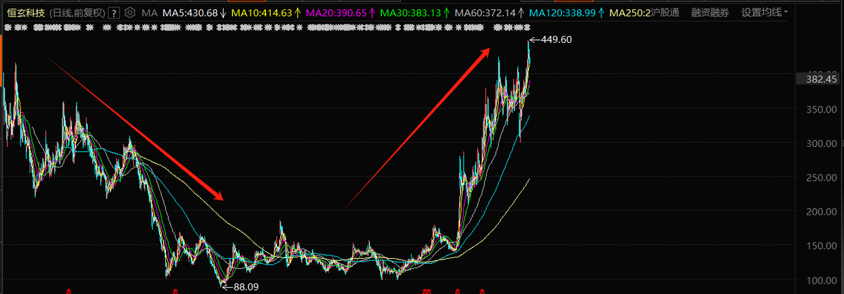
Furthermore, the capital market's enthusiasm for the InP sector continues to rise, becoming an important indicator of the industry's prosperity. US-listed AXT's stock price has surged by 1000% in the past six months, with its indium phosphide (InP) business revenue increasing by over 250% quarter-on-quarter and backlogged orders reaching nearly $50 million. Lumentum, a leading optical chip manufacturer, is operating its InP production lines at full capacity, and related A-share listed companies like Yunnan Germanium have also seen valuation recovery. After an initial broad-based rally, the market is gradually moving towards value differentiation, with technological strength, customer certification progress, and CPO suitability becoming the core valuation logic.
In summary, amidst the explosive growth of AI computing power and the intertwining of global technological competition, competition in the InP market has become a key bargaining chip in the great power game and a crucial battle for my country to achieve a "leapfrog development" in the semiconductor field. Breakthroughs in the InP industry not only solve the "bottleneck" problem in photonic chips but also reshape the global industrial competitive landscape through full-chain localization. With the large-scale application of 6-inch process technology, China is expected to occupy 30% of the global InP market by 2030, propelling strategic industries such as optical communication and quantum computing into a "China-led era."
Undercurrents are brewing
Indium phosphide: Technological challenges and supply chain security
Despite indium phosphide's (IPP) superior performance placing it at the forefront of AI and optical communication development, its industrialization and large-scale commercialization still face significant technological and cost challenges that urgently need improvement.
Industry experts point out that, firstly, the "black box" effect at the process level restricts the rapid release of production capacity. The core pain point in the IPP supply chain lies in the crystal growth stage. The currently mainstream vertical gradient solidification (VGF) process is extremely complex. Because the crystal must grow in a sealed, high-temperature, and high-pressure extreme environment, the entire process is like an invisible "black box," making the adjustment and optimization of process parameters extremely difficult. This process is highly prone to crystal defects such as twins, resulting in drastic fluctuations in yield and a generally low yield rate, ranging from single digits to 40%, becoming the primary technological barrier restricting stable and rapid capacity release.
These technological challenges further extend to the commercialization level, directly driving up product costs and prices. Currently, the price of indium phosphide (InP) substrates is significantly higher than that of silicon and gallium arsenide (GaAs) materials. The price of a 6-inch RF-grade InP substrate has risen to 18,000 yuan per piece. While this high cost is acceptable in cutting-edge computing infrastructure where cost is no object, it makes it difficult to penetrate price-sensitive mass markets such as consumer electronics, thus limiting market expansion.
Faced with these challenges, the industry is seeking a breakthrough through technological evolution and specification upgrades. Increasing wafer size is one of the core paths to cost reduction. The transition from the current mainstream 4-inch wafers to 6-inch and even larger sizes can significantly increase the number of chips produced per wafer, thus reducing manufacturing costs. Simultaneously, continuously optimizing crystal growth processes, improving yield rates, and achieving the localization of key production equipment are all ways to overcome the cost constraints and lay the foundation for wider commercial applications in the future.
Furthermore, it is worth noting that the rapid development of the indium phosphide industry is also overshadowed by geopolitical competition and export controls.
Today, indium has been listed as a critical mineral by China, the US, Europe, Japan, and other countries, further highlighting the strategic value of indium phosphide in global technological competition. This material, possessing high frequency, high speed, low power consumption, and radiation resistance, has become a key bargaining chip in the technological competition among major powers.
In February 2025, China imposed export controls on strategic minor metals such as indium. As the supplier of more than 50% of the world's indium resources, this policy, while preventing the outflow of strategic resources and forcing the industrial chain to upgrade to higher value-added segments, also intensifies the global supply chain restructuring game.
The United States, through CFIUS reviews, has strengthened its control over Chinese high-tech investments. Recently, it forcibly halted Hanfu Optoelectronics' acquisition of the US company Emcore with an executive order. The transaction, valued at only $2.92 million, has attracted significant attention due to its involvement in indium phosphide technology, primarily due to concerns about the strategic nature of indium phosphide. The US, citing "national security," determined that Emcore's indium phosphide technology, embedded in the US defense supply chain, could potentially endanger national security. This case highlights that US reviews of Chinese high-tech investments have transcended commercial logic, exhibiting a pervasive focus on security.
This geopolitical game has brought uncertainty to the global indium phosphide industrial chain. On the one hand, export controls may lead to supply chain fluctuations and affect the release of global production capacity; on the other hand, they also force countries to strengthen the construction of their local industrial chains and promote the restructuring of the global industrial landscape.
In Conclusion
Looking at the big picture, indium phosphide (IPP), with its irreplaceable physical properties in high-frequency and high-speed applications, coupled with the rigid demand from industries such as AI computing power, CPO, high-speed optical communication, and LiDAR, has officially moved beyond its niche positioning and become a strategic core material supporting global AI computing power and optical communication networks, ushering in a critical turning point for large-scale commercialization.
Looking ahead, the IPP industry is on the eve of a large-scale explosion. Although it currently faces development bottlenecks such as low crystal growth yield and high costs, and is heavily influenced by uncertainties such as geopolitical competition and export control adjustments, the global expansion wave and the breakthrough of domestic production by Chinese companies have created a synergy. With the continuous increase in production capacity and the continuous breakthroughs in key technologies such as substrates, this niche market will usher in a historic growth opportunity.
Source: Semiconductor Industry Observer